Perovskite optoelectronic devices and physics
2019, 68 (15): 158506.
doi:10.7498/aps.68.20190675
Abstract +
When there is a strong spin-orbit coupling in some direct semiconductor with an inversion-asymmetric structure, the Rashba effect will exist, splitting the spin-degenerated bands into two sub-bands with opposite spin states. These two sub-bands will deviate from the symmetry center of the Brillouin zone, making the semiconductor an indirect band gap semiconductor. Metal halide perovskites exhibit strong spin-orbit coupling and possess an inversion-asymmetric crystal structure, showing great potential in Rashba effect research. In this review, we systematically review the Rashba effects in perovskites, including the theoretical and experimental studies for demonstrating the Rashba effect in perovskites, the influence of Rashba effect on the carrier recombination, and the current debates concerning the Rashba effect in perovskites. Then, several problems that need to be solved urgently are proposed,they being 1) whether there exists the Rashba effect in the perovskite, 2) whether the Rashba effect can exert a significant influence on carrier recombination, and 3) what the relationship between the Rashba effect and the perovskite stucture is. The prospects are also given for the future research including the study of the Rashba effect in perovskites by various spectral methods and the applications of the Rashba effect in optical-electronic-magnetic devices.
2019, 68 (15): 157101.
doi:10.7498/aps.68.20190596
Abstract +
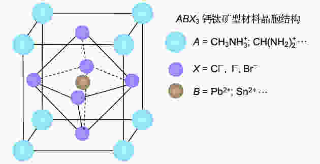
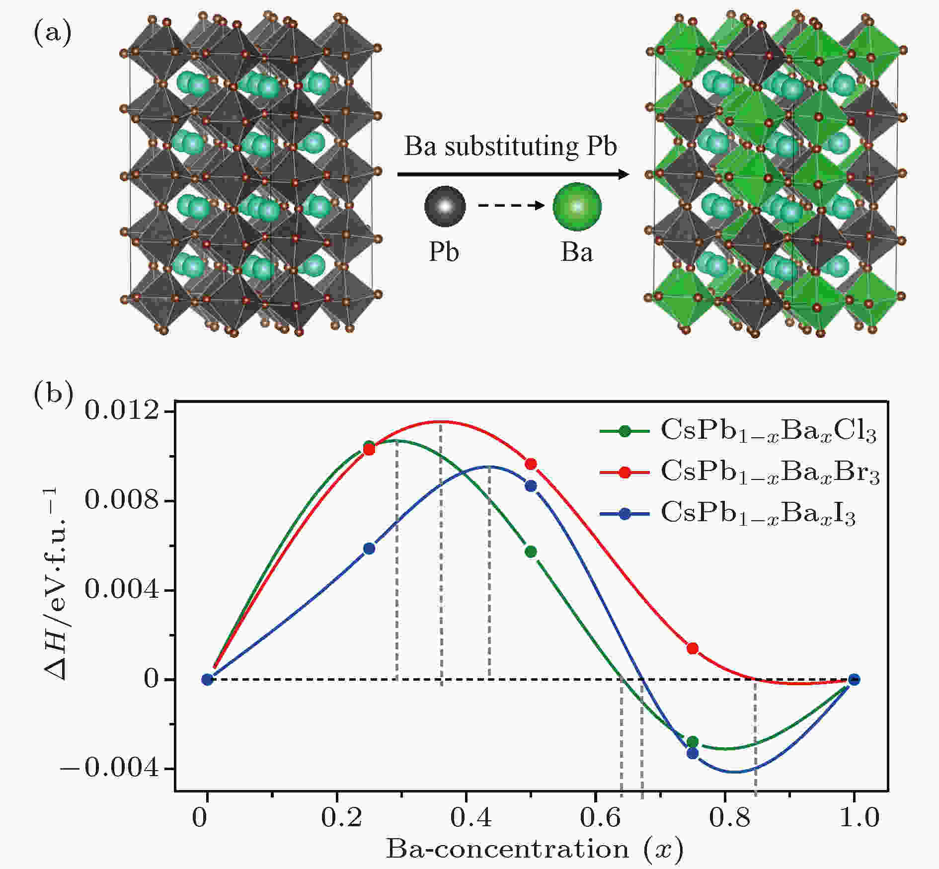
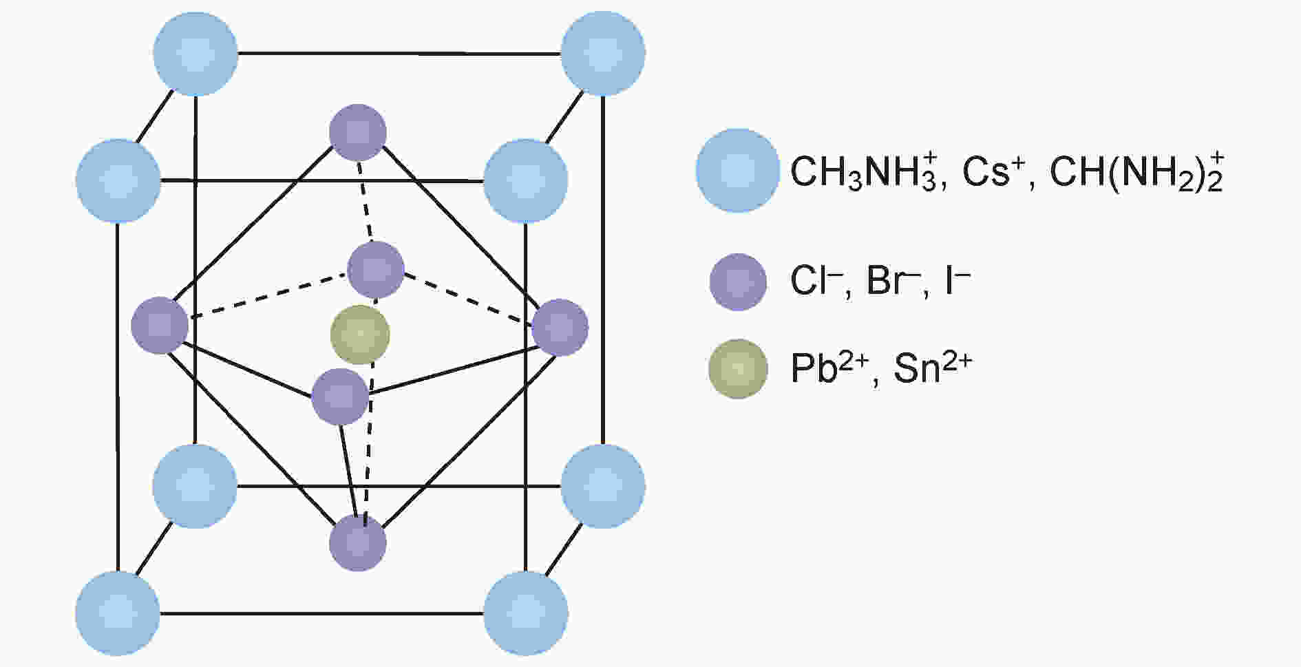
Organic-inorganic halide perovskitesABX3(A= CH3NH3, HC(NH2)2;B= Pb;X= Cl, Br, I) have recently attracted increasing attention due to their advanced optoelectronic properties. However, the poor stability and toxicity of organic lead halogen perovskites are still a major challenge for deploying the outdoor solar cells. Element substitution is a simple and effective strategy to solve these problems. For example, the substitution of the I ions with Cl and Br has been regarded as a reliable method to improve the device stability.A-site engineering, i.e., replacing organic ions with inorganic cations (such as Cs+, Rb+), has also been reported. TheB-site alloying approach has been demonstrated with Zn, Sr, Sn, etc. Inorganic halide perovskites can be synthesized by the low-cost solution spin-coating method and have similar optoelectronic properties and improved stability to their organic counterparts. Here in this paper, we report a comprehensive study of the alloyed perovskite CsPb1–xBaxX3(X= Cl, Br, I) by combining the disorder alloy structure search method with first-principles energy calculations. We find that it is not easy to dope barium into the perovskite lattice when Ba concentration is low and the stable disordered solid solution can exist in the high Ba concentration case. Carrier effective mass and bandgap increase with the increase of Ba concentration and the bandgap change range is wide, owing to the difference in both electronegativity and ionic radius between Pb and Ba. After inducing Ba into CsPb1–xBaxX3(X= Cl, Br, I), the higher electron concentration on the I sites also enhances the Coulomb interaction of the Pb—I bonds. Moreover, the electrons and holes tend to be located on Pb sites, and this may give rise to the formation of local potential wells, which would further induce the large lattice deformation to accommodate the self-trapped excitons. Especially, CsPbI3-Pnmaperovskite is metastable in the ambient environment with a suitable photon absorption threshold. The CsPb1–xBaxI3can be used as a capping layer on CsPbI3in solar cells, thereby significantly improving the power conversion efficiency and long-term stability. Overall, the alloyed perovskite CsPb1–xBaxX3(X= Cl, Br, I) with high Ba concentration can be stable and less-toxic, and they can be used in short wave light-emitting diodes, radiation detectors or other fields because of their large bandgaps (> 2.8 eV).
2019, 68 (15): 157102.
doi:10.7498/aps.68.20190324
Abstract +
Lead halide perovskites, which can be grown by solution process, are very suitable for various optoelectronic applications, such as in solar cells, light-emitting diodes, lasers and photo-detectors, due to their outstanding electrical and optical properties. However, lead halide perovskites are unstable under continuous light illumination, which severely degrades the performance and lifetime of optoelectronic devices based on them. Therefore, the photo-stability of perovskites and the mechanisms have received more and more attention. In this article we review the main phenomena in perovskites, induced by continuous light illumination, namely photo curing, photo dissociation, photo-induced phase separation, and photo-induced phase transition. The proposed mechanisms for the instability from the perspectives of defect states, ion migration, thermodynamics and chemical bonds, respectively, are also introduced. Finally, the complexity presented in the studying of photo-stability, and the issues should be addressed in the future are also briefly discussed.
2019, 68 (15): 158401.
doi:10.7498/aps.68.20190569
Abstract +
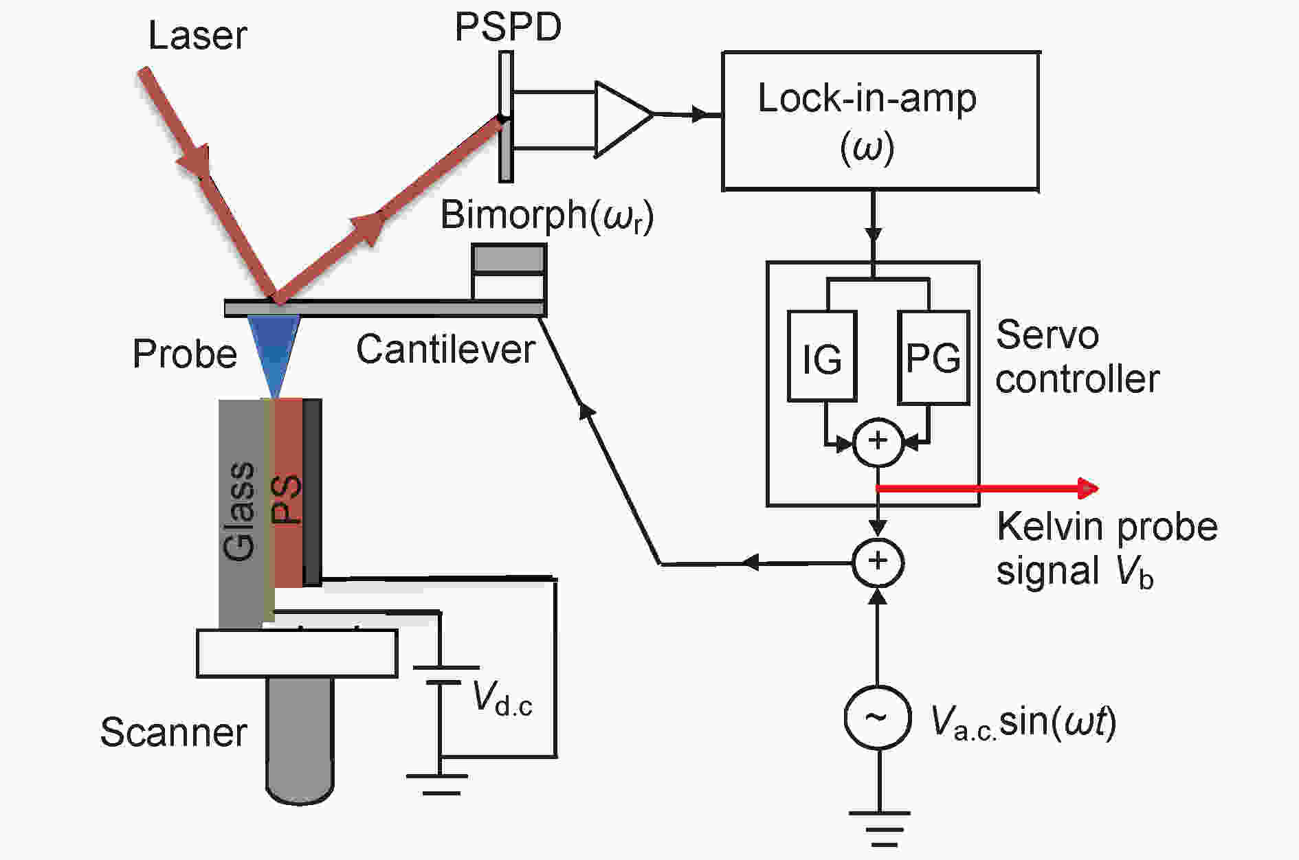
Perovskite solar cells, as a promising next-generation photovoltaic technology for large-scale application, have demonstrated the advantages of high absorption coefficient, tunable bandgap, considerable photoelectric conversion efficiency and low-cost fabrication. However, the photoelectric conversion process within the device is still not understood clearly. One of the major reasons is that it is difficult to directly observe the space potential inside the device and its effect on the photogenerated charge carriers. The direct measurement and analysis of the space potential inside the device and the clarification of the intrinsic relationship between the space potential and the charge carrier micro-process under illumination and different electric field conditions can reveal the photoelectric conversion mechanism in depth, and thus providing the scientific research basis for the further development. Kelvin probe force microscopy (KPFM), a testing technology that is non-contact, can detect the space potential distribution without any damage to the device, demonstrating the great potential to unveil the working mechanism of perovskite solar cells accurately. Such a characterization method can work under vacuum condition. The KPFM combines Kelvin method of measuring contact potential difference with the scan probe microscopy to characterize internal carrier dynamic behavior with high resolution on a nanometer scale. The study of the spatial potential distribution of semiconductor device plays an important role in understanding the working mechanism of new perovskite solar cells. For example, under an open-circuit condition, the intensity and width of the electric field and space charge region can be obtained from the spatial potential distribution, and the bending direction of the energy band can be judged according to the increase or decrease of the potential. While in a short-circuit case, the generation and transport of charge carriers can be obtained. In this review, we mainly introduce the research progress of the space potential distribution and optoelectronic conversion mechanism in perovskite solar cells. The key mechanism of charge carrier generation, separation, transport and recombination are revealed by using KPFM to directly observe the space potential variations caused by light or electric field. We also prospect the issues and challenges in the future research.
2019, 68 (15): 158503.
doi:10.7498/aps.68.20190745
Abstract +
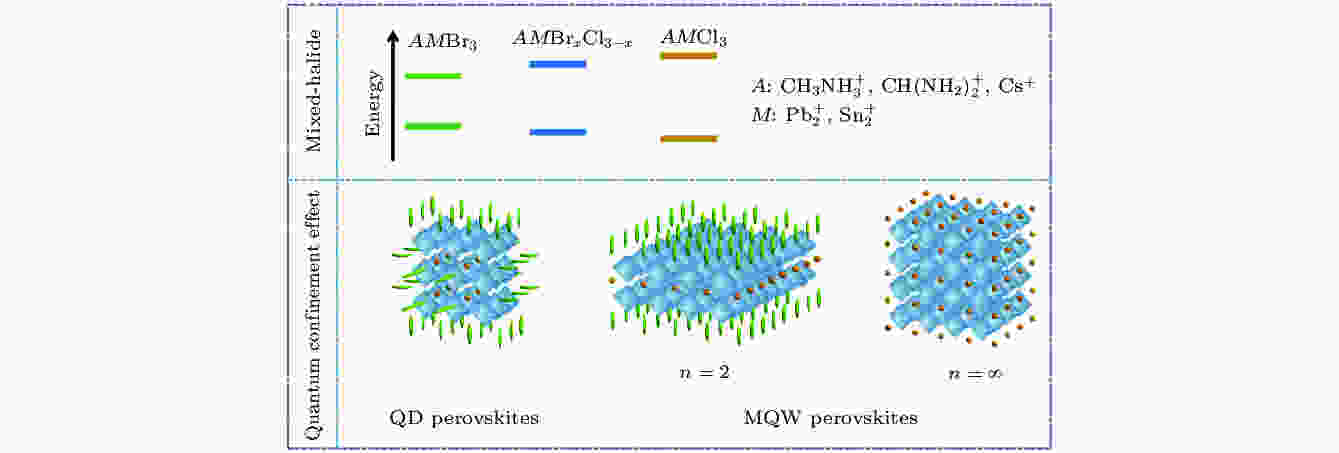
The great progress of light-emitting diodes (LEDs) has been made based on perovskites, and the external quantum efficiency of near infrared, red and green devices have reached > 20%, exhibiting their great potential applications in lighting and displays. However, the performance of blue perovskite LEDs is very poor, thus limiting their applications in the field of full-color displays. The blue perovskite LEDs can be achieved through mixed halides or quantum confinement effect. In this paper, we review the research progress of blue perovskite LEDs based on these two strategies, discuss the challenges to achieve high-performance perovskite LEDs and present our perspectives.
2019, 68 (15): 158504.
doi:10.7498/aps.68.20190647
Abstract +
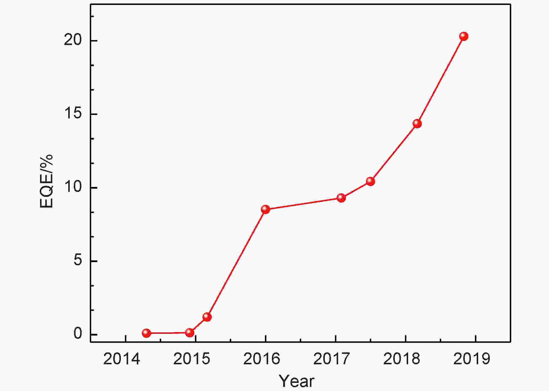
Perovskite light emitting diodes exhibit the advantages of high color purity, tunable wavelength and low producing cost. Considering these superiorities, one regards perovskite light emitting diodes as very promising candidates for solid state lighting and panel displaying. Human eyes are very sensitive to green light, thus green perovskite light emitting diodes receive the most attention from researchers. Since the advent of the very first green perovskite light emitting diode, the external quantum efficiency has climbed from only 0.1% to over 20%. In this review, we mainly discuss the history of green perovskite light emitting diodes, the basic concepts of perovskite materials and green perovskite light emitting diodes, and the common methods to improve the efficiency of green perovskite light emitting diodes. The bandgap of bromide perovskite is about 2.3 eV, which is located just on a green light wavelength scale and thus becomes the suitable emitting layer material for green emission. There are mainly two types of device structures, i.e. regular format and inverted format. The whole working process of green perovskite light emitting diodes can be divided into two stages, i.e. the injection and recombination of charge carriers. One engineers the energy levels of different layers to improve the injection of charge carriers. They also raise up the strategy so-called surface passivation to reduce the defect density at the interface in order to avoid the quenching phenomenon. One usually inserts a buffering layer to realize the surface passivation. Besides, perovskites possess very small exciton binding energy, which is at the same order of magnitudes as the kinetic energy at room temperature. Charge carriers become free in this case, which will severely reduce the radiation recombination probability due to the non-radiation recombination process such as Shockley-Read-Hall effect and Auger recombination. To solve the problem, people fabricate three types of perovskites, namely quasi two-dimensional perovskite, perovskite quantum dot, and perovskite nanocrystal. In this way, the charge carriers can be confined into a limited space and the exciton binding energy will hence be improved. From the efficiency perspective, the green perovskite light emitting diodes promise to be commercialized. However, another critical issue impeding the development of green perovskite light emitting diodes is the stability problem. Comparing with the organic light emitting diodes and inorganic quantum dot light emitting diodes, the lifetime of perovskite light emitting diodes is too limited, which is only approximately one hundred hours under normal conditions. The temperature, moisture and light exposure are all factors that influence the stability of perovskite light emitting diodes.
2019, 68 (15): 158505.
doi:10.7498/aps.68.20190307
Abstract +
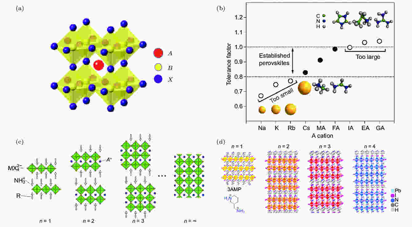
In recent years, metal halide perovskites have received extensive attention due to their superior optoelectronic properties and solution processability, which also become a research hotspot in the field of optoelectronics. Among all the perovskite optoelectronics applications, perovskite light-emitting diode (LED) becomes one of the important research topics because it is likely to be used in the next-generation display technique. Based on the high photoluminescence quantum yield (PLQY), facilely tunable bandgaps, and sharp emission of perovskite material, the external quantum efficiency of perovskite LED has increased from less than 1% to over 20% within only five years, showing the most rapid development speed in the LED field. During the 5-year exploration of perovskite LEDs, researchers have focused their efforts on how to realize the crystal-growth control in the perovskite film formation process, enhance PLQY of the perovskite films, and improve the performance of perovskite LEDs. Among all the approaches, the utilization of organic additives including small molecules and polymers proves to be an effective strategy. Here, in this article, we review the recent advances in metal halide perovskite LEDs based on the strategy of organic-additive treatment. We also analyze and discuss the interaction between organic additive and perovskite crystal as well as its influence on the performance of perovskite LED. In the end, we discuss the challenges remaining in perovskite LEDs and the prospects for perovskite LEDs.

2019, 68 (15): 158801.
doi:10.7498/aps.68.20190853
Abstract +
In recent years, metal halide perovskite solar cells have attracted widespread attention due to their unique technological superiority. Remarkable progress of device performance has been achieved in last few years. The certified efficiency has reached 24.2%, which is close to the efficiency of the commercial crystalline silicon solar cells. Halide perovskite is a kind of semiconductor and ionic conductor material, which not only has the ability to transfer charges, but also exhibits the phenomenon of ion migration under an external electric field. Ion migration can directly change the local chemical ratio of perovskite crystals, and can also greatly affect the electrical properties of materials and the working mechanisms of corresponding devices. In this review, the formation mechanism, basic characteristics and effects of ion migration on the working mechanism of the device (such as giant switchable photovoltaic phenomenon, current hysteresis, etc.) are summarized, and then some recent advances in the suppression of ion migration are introduced. Since there exist still many doubts about ion migration in perovskite materials, it is very important to understand the phenomenon of ion migration in perovskite materials in order to promote the development and application of perovskite solar cells.
2019, 68 (15): 158802.
doi:10.7498/aps.68.20190306
Abstract +
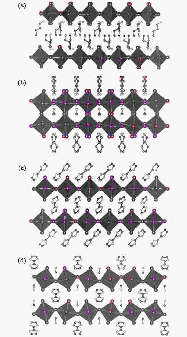
Hybrid perovskites are a series of solution-processable materials for photovoltaic devices. To achieve better performance and stability, interface passivation is an effective method. So far, the most commonly used passivators are organic amines, which can tailor perovskite into a lower-dimensional structure (Ruddlesden-Popper perovskite). Here, we select a biimizole (BIM) molecule as a new passivator for perovskite. The BIM based single layer perovskite has a more rigid structure. And multi-layered structure cannot be formed due to large lattice mismatching and structural rigidity. By inducing the excess MAI (methanaminium iodide) into the lattice, the layered structure is maintained, and half of the BIM molecules are replaced by MA (methylamine). The mixed layered structure is distorted, because of the difference in size between two kinds of cations. We then investigate passivation effect of BIM on perovskite solar cells. By carefully controlling the feed ratio in precursor solutions, we fabricate solar cells with different passivation structures. We find that the introduction of BIM can causeVocto increase generally, indicating that MAPbI3is well passivated. The peak at 7.5° and 15° in X-ray diffraction pattern are corresponding to a two-dimensional (2D) phase with a shorter layer distance. There are no peaks at lower degrees, so that no multi-layered structure is formed in the film either. We suppose that a dual-phase 2D-3D (where 3D represents three-dimensional) structure is formed in the perovskite film. To explain the passivation effect of the two 2D structures, we investigate their lattice matching towards MAPbI3. The distorted 2D structure is well matched with (110) face of o-MAPbI3, and the mismatching rate is lower 1% in the two directions. On the other hand, the BIM based 2D structure cannot well match with (–110) face of o-MAPbI3, nor with (001) face of c-MAPbI3. We also consider that the less rigidity of distorted structure contributes to better passivation. As a result, we achieve a BIM passivated perovskite solar cell with a power conversion efficiency up to 14%. This work paves a new way to the interface engineering of perovskite solar cells.
2019, 68 (15): 158803.
doi:10.7498/aps.68.20190468
Abstract +
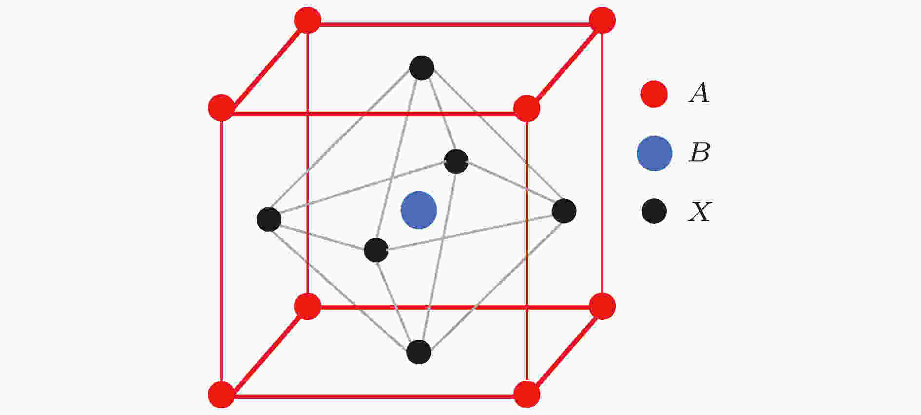
In recent years, organic-inorganic hybrid perovskite solar cells have aroused the interest of a large number of researchers due to the advantages of large optical absorption coefficient, tunable bandgap and easy fabrication. Recently, the power conversion efficiency of organic-inorganic hybrid perovskite solar cells has been enhanced to more than 23% in laboratory. In solution processed perovskite solar cells, perovskite and charge transport layer are stacked together, due to the different crystallization rates leading to lattice mismatch near the surface region of perovskite film, resulting in a lot of interface defects, especially at the interface between perovskite and charge transport layer. What is more, the photo-induced free carriers must transfer across the interfaces to be collected. But the defects near the interface can trap photogeneration electrons, thus reducing the carrier lifetime and causing the charges to be recombined, which greatly influence the performance and stability of perovskite solar cells. Therefore, reducing and passivating these defects is critical for obtaining the high performance perovskite solar cells. Now, there have been made tremendous efforts devoting to advancing passivation techniques, such as doping and surface modification, for high efficiency perovskite solar cell with improved stability and reduced hysteresis. These approaches also contribute to improving the energy band alignment between carrier transport layers and perovskite absorber improving device performance, or resistance moisture to enhance device stability. In this review we mainly introduce the formation and the effect of defects on perovskite solar cells, analyze the mechanism for passivating the interfacial defects between charge transport layer and perovskite photo absorption layer for different materials, compare the effects of different passivation materials on the photovoltaic performance of perovskite solar cells, and summarize the role of these materials in passivating the defects. Finally we discuss the research trend and development direction of passivation defects in perovskite solar cells.
2019, 68 (15): 158804.
doi:10.7498/aps.68.20190343
Abstract +
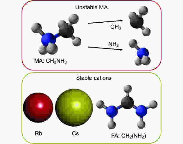
The power conversion efficiency of organic-inorganic hybrid perovskite solar cell has exceeded 24%. The rapid increase in efficiency coupled with its cost-effective fabrication has attracted tremendous attention toward the commercialization of perovskite solar cells. The biggest challenge that hinders the commercialization of perovskite solar cells is the long-term instability of materials and the corresponding devices, which cannot compete with other commercialized solar cells, such as Si cells, in terms of lifetime. The intrinsic instability of perovskite material itself is the most critical challenge faced by researchers. In this study, we discuss the intrinsic instability of organic-inorganic hybrid perovskite materials from the aspects of both chemical instability and phase instability. Suggestions for improving the stability of perovskite solar cell are provided from the perspective of composition design and fabrication process.
2019, 68 (15): 158805.
doi:10.7498/aps.68.20190303
Abstract +
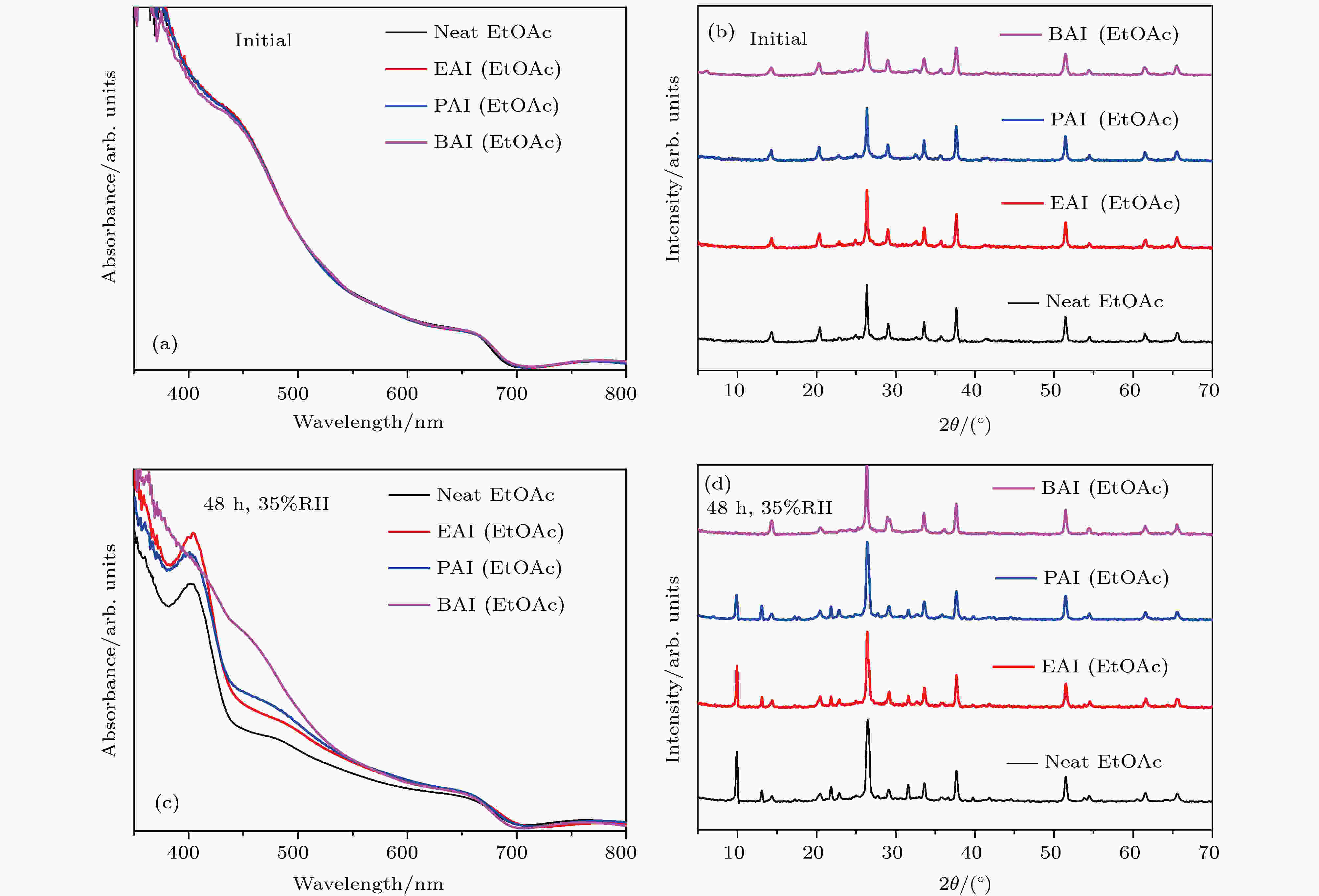
All-inorganic perovskite cesium lead halides with superior stability, suitable bandgap and high absorption efficient have become a promising candidate for photovoltaic application. In all-inorganic cesium lead halide perovskites, CsPbX3(X= Br, I) exhibits excellent photoelectric properties, which are similar to those of organic-inorganic hybrid perovskites. The CsPbI3faces a challenge of unideal tolerant factor for perovskite phase while CsPbI3–xBrxhas better tolerant factor. Among them, CsPbI2Br is one of most popular candidates because of its good thermal stability. Nevertheless, CsPbI2Br shows instability due to the phase transition caused by moisture and lower efficiency because of defects. For all inorganic perovskite devices, the alkyl chain length of surface treatment agent should be taken into account when using organic cationic passivation method. In this paper, CsPbI2Br perovskite is treated with different organic ammonium salts to enhance its phase stability. The experimental results show thatα-phase CsPbI2Br is more stable with the increase of the alkyl chain length. Butylamine iodine (BAI) among three kinds of surface treating agents is proved to have the best defect passivation and phase stabilization effect. With the increase of alkyl chain length, the hydrophobicity of the organic molecular layer increases, which plays a crucial role in protecting optically active CsPbI2Br. Meanwhile, it is found that the stability of perovskite is enhanced with the concentration of the BAI solution increasing. This should be related to the organic cation termination formed on the surface of CsPbI2Br film. Solar cell devices based on the CsPbI2Br thin films treated with different concentrations of BAI are assembled and then the effect of organic ion surface treatment on the photoelectric performance of batteries is further explored. The experimental results show that when the concentration of BAI is relatively high (4 mg/mL and 8 mg/mL), the device’s photovoltaic performance decreases especially the photocurrent obviously decreases, while the post-treatment process using 2 mg/mL BAI will enhance not only the phase stability but also the photovoltaic parameters after defect passivation. Considering both humidity resistance and device efficiency, this work demonstrates that the CsPbI2Br thin film with suitable BAI treatment can improve the wet stability of perovskite, and enhance the photovoltaic performance.
2019, 68 (15): 158806.
doi:10.7498/aps.68.20190355
Abstract +
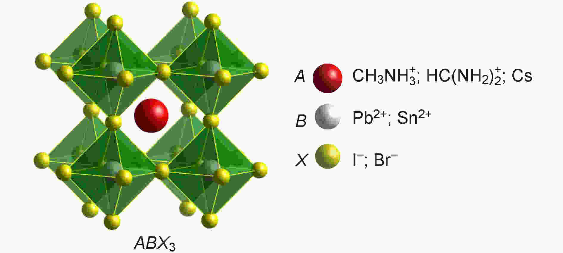
Photovoltaic technology, which can converse solar illumination into electricity, is crucial to the sustainable development of human civilization. Among them, the organic-inorganic hybrid perovskite solar cell (OIPSC) has become a research front due to its excellent photoelectric characteristics, low production cost and high power conversion efficiency (PCE). Although the PCE of OIPSC has exceeded 24%, the organic components in the perovskite system are sensitive to the decomposion caused by either being exposed to light or heated in high temperature environment. The stability defects have greatly limited the commercialization of perovskite solar cells. Therefore, it is urgent to improve the stability of perovskite solar cells, especially to solve the material decomposition problem. All-inorganic perovskite photovoltaic material, composed of all-inorganic elements, exhibits excellent heat and moisture resistance. Therefore, the development of all-inorganic perovskite solar cells is of great significance for solving the current stability problems in perovskite photovoltaics. In this work, we review the recent research progress of all-inorganic perovskite solar cells, discuss the solution approaches to processing all-inorganic perovskite films, and explore the enhancement of device stability. Our work provides a guideline for further promoting the device stability and PCE.

2019, 68 (15): 158807.
doi:10.7498/aps.68.20190302
Abstract +
In the field of photovoltaic materials, perovskite has attracted extensive attention during the past years, owing to its excellent photovoltaic properties, including high charge carrier mobility, low exciton binding energy, long charge carrier diffusion length, broad light absorption spectrum, large absorption coefficient, and low-cost solution processability. However, due to the limitations of film preparation methods (typical spin coating), industrial large-scale production of perovskite solar cells is still in infancy. The inkjet printing technology is a significant manufacturing technology developed from home and office printing and widely used in various printing electronics industries. Compared with other deposition methods, it possesses many advantages, including low cost, high material utilization, high patterning precision, etc. As a direct writing technology, the inkjet printing has shown great industrial potential and is expected to be employed in the industrialization of perovskite solar cells. In this paper, we review the research progress of perovskite solar cells fabricated via the inkjet printing and the application of inkjet printing technology to various functional layers (electrode, hole transport layer, electron transport layer, perovskite active layer). Finally, the challenges of inkjet printed perovskite solar cells at this stage are discussed, and the commercialization direction of inkjet printed perovskite solar cells is also pointed out.


