


Vol. 73, No. 13 (2024)
2024-07-05
The 90th Anniverary ofActa Physica Sinica·COVER ARTICLE
COVER ARTICLE
The 90th Anniverary ofActa Physica Sinica·COVER ARTICLE
COVER ARTICLE
2024, 73 (13): 138701.
doi:10.7498/aps.73.20240592
Abstract +
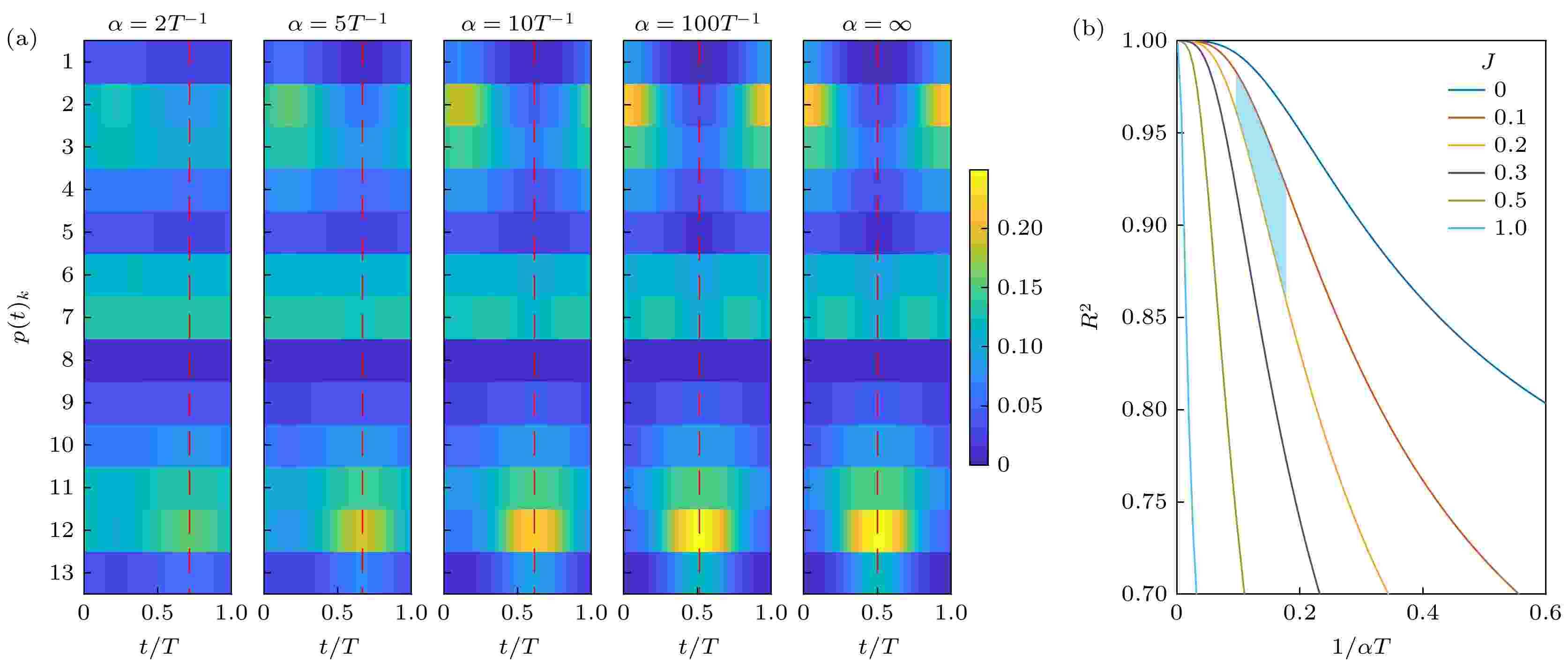
A comprehensive description of the protein should include its structure, thermodynamics, and kinetic properties. The recent rise of cryogenic electron microscopy (cryo-EM) provides new opportunities for the thermodynamic and kinetic research of proteins. There have been some researches in which cryo-EM is used not only to resolve the high-resolution structure of proteins but also to analyze the conformational distribution of proteins to infer their thermodynamic properties based on data processing methods. However, whether cryo-EM can be used to directly quantify the kinetics of proteins is still unclear. In this work, an ideal protein system, cyanobacterial circadian clock protein, is selected to explore the potential of cryo-EM used to analyze the non-equilibrium process of proteins. Previous research has illustrated that cryoelectron microscope can be used to infer the thermodynamic information about the KaiC protein such as the inter-subunit interaction within the hexamers. Herein, we extend the equilibrium Ising model of KaiC hexamers to a non-equilibrium statistical physics model, revealing the properties of the non-equilibrium process of KaiC hexamers. According to the non-equilibrium model and previous biochemical research, we find that the intrinsic properties of KaiC protein allow its non-equilibrium conformational distribution to be measured by cryo-EM.

Instrumentation and Measurement
EDITOR'S SUGGESTION
2024, 73 (13): 130702.
doi:10.7498/aps.73.20240560
Abstract +
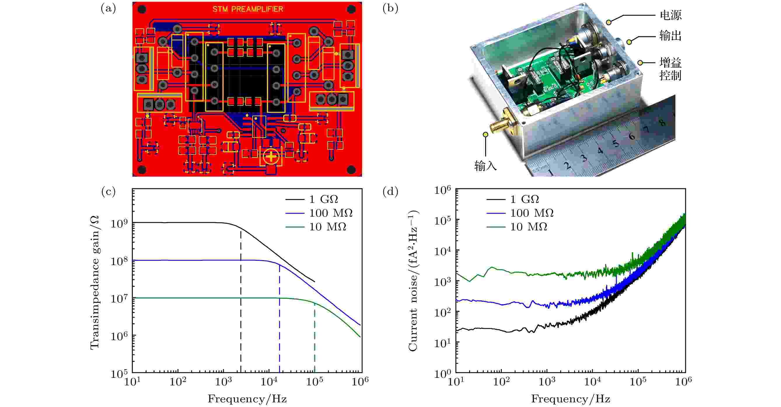
The current preamplifier is one of the important components of the scanning tunneling microscope (STM), and its performance is crucial to the basic operations of the STM system, as well as for the development of demanding novel functionalities such as autonomous atomic fabrication. In this study, the factors that affect the performance of a current preamplifier, including its noise spectrum density and the bandwidth, are analyzed in depth, and a preamplifier is designed and fabricated specifically for the STM system. By using a carefully selected low-noise op amp chip, the optimized current preamplifier has a noise floor as low as 4
$ {\mathrm{f}}{\mathrm{A}}/\sqrt{{\mathrm{H}}{\mathrm{z}}} $
and a bandwidth of 2.3 kHz, at its most sensitive transimpedance gain of 1 GΩ. It has three transimpedance gains, 10 MΩ, 100 MΩ, and 1 GΩ, that can be switched through digital control signals. A two-switch configuration is adopted to minimize the noise floor while maintaining the optimal bandwidth. The current detectable by this three-level preamplifier ranges from pA to μA, satisfying the requirements of most STM operations. Using this preamplifier, the fundamental functions of the STM system are successfully demonstrated, including surface topographic characterization, scanning tunneling spectroscopy, and single atom/molecule manipulation. The measurement of shot noise in tunneling current is also explored, and a linear relationship between shot noise and tunneling current is obtained by carefully analyzing noise. It is illustrated that the Fano factor of the shot noise in a normal metallic tunneling junction is approximately equal to 1, revealing the expected Poisson process for electron tunneling in such a scenario. The results are valuable for the high-resolution characterization of correlation systems in the future.

REVIEW
EDITOR'S SUGGESTION
2024, 73 (13): 136101.
doi:10.7498/aps.73.20240541
Abstract +
Ion irradiation, a technology in which ion beams are used to irradiate materials, has high manipulation precision, short processing time, and many applications in the fields of material modification, chip manufacturing, biomedicine, energy and chemicals. Especially in magnetic material modification, customized modifications of magnetic materials can be achieved by precisely controlling the energy, dose, and direction of the ion beam. To further enhance the performances of magnetic materials and explore new magnetic devices, this study focuses on how ion irradiation precisely modulates various magnetic interactions and the analysis of its influence on the spin Hall effect and magnetic structural dynamics. Firstly, the latest research achievements are emphasized of ion irradiation regulated magnetic characteristics such as perpendicular magnetic anisotropy, exchange bias, and RKKY interaction. These regulation methods are crucial for understanding and optimizing the microstructure and properties of magnetic materials. Secondly, the significant role played by ion irradiation in regulating spin-orbit torque devices is discussed in detail. These applications demonstrate the potential of ion irradiation technology in designing high-performance magnetic storage and processing devices. Finally, the future applications of ion irradiation technology in the preparation of multifunctional magnetic sensors and magnetic media for information storage are discussed, highlighting its great enormous innovation and application potential in the field of magnetic materials.
GENERAL
2024, 73 (13): 130201.
doi:10.7498/aps.73.20240239
Abstract +
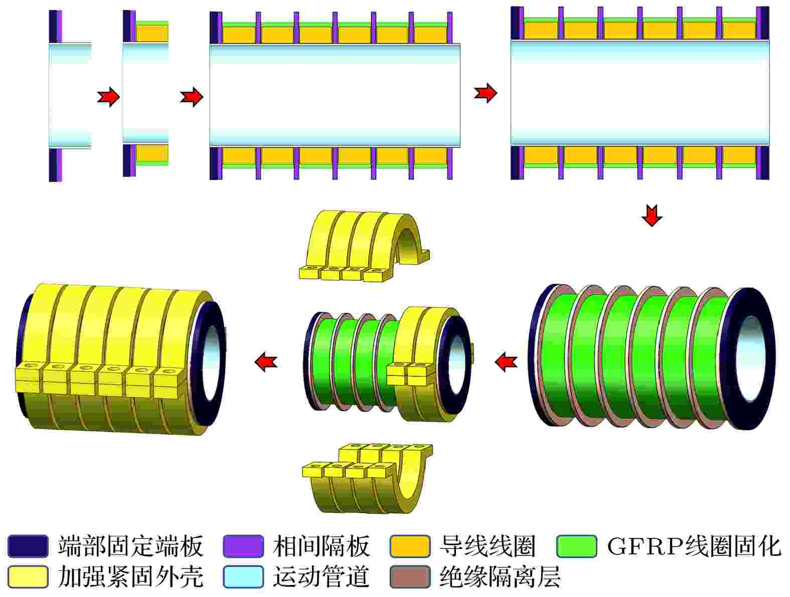
In order to alleviate the common problems of skeleton fracture and failure in traditional propulsion systems, the insulation degradation and structural instability existing in integrated drive structures during operation are investigated in this work. By using stress-strain calculations of a typical integrated drive structure and voltage-withstanding discharge tests after acceleration experiments, key factors are identified, and it is believed that the tensile stress inside the driving structure is one of the reasons for structural instability. Owing to the electromagnetic force acting on the coil, the integrated driving structure exhibits high tensile stress and strain on the inner wall and interphase partition, accompanied by significant deformation, which is not conducive to the overall structural stability. Based on the above calculation results, a novel modular drive structure with bidirectional separation is proposed, which can realize the radial separation between the phase partition and the skeleton inner cylinder, as well as axial separation between different driving coils. Finite element simulation analysis is conducted to evaluate its acceleration performance and structural response during operation. The results indicate that under the same excitation conditions, the new driving structure greatly reduces the interaction between the coil and the inner wall during operation, so the stress-strain on the inner wall of the new driving structure is much smaller than that of the integrated structure. The maximum deformation decreases from approximately 10–2m in the integrated structure to about 10–5m to 10–6m in the new design. These findings emphasize the potential of new structure to improve reliability while ensuring propulsion performance, providing valuable insights for optimizing electromagnetic coil drive structures. For this new structure, there will be plans to conduct high-pressure propulsion experiments in the future to verify its reliability.
2024, 73 (13): 130501.
doi:10.7498/aps.73.20231888
Abstract +
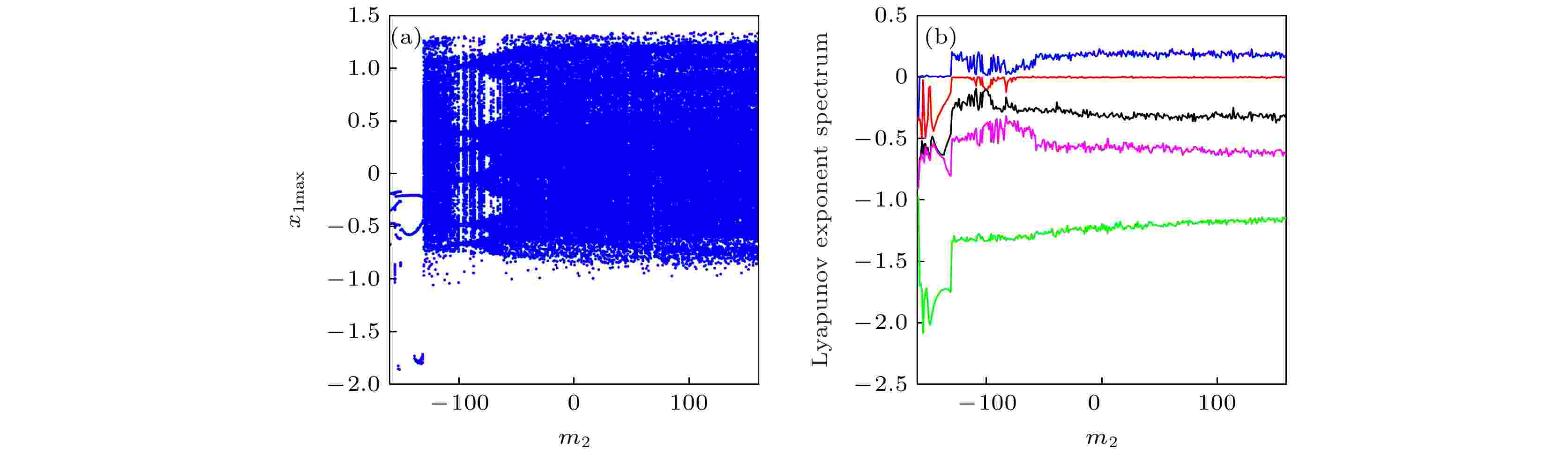
The neural network model coupled with memristors has been extensively studied due to its ability to more accurately represent the complex dynamic characteristics of the biological nervous system. Currently, the mathematical model of memristor used to couple neural networks mainly focuses on primary function, absolute value function, hyperbolic tangent function, etc. To further enrich the memristor-coupled neural network model and take into account the motion law of particles in some doped semiconductors, a new compound exponential local active memristor is proposed and used as a coupling synapse in the Hopfield neural network. Using the basic dynamic analysis method, the system’s dynamic behaviors are studied under different parameters and the coexistence of multiple bifurcation modes under different initial values. In addition, the influence of frequency change of external stimulation current on the system is also studied. The experimental results show that the internal parameters of memristor synapses regulate the system, and the system has a rich dynamic behavior, including symmetric attractor coexistence, asymmetric attractor coexistence, large-scale chaos as shown in attached figure, and bursting oscillation. Finally, the hardware of the system is realized by the STM32 microcontroller, and the experimental results verify the realization of the system.
EDITOR'S SUGGESTION
2024, 73 (13): 130502.
doi:10.7498/aps.73.20240739
Abstract +
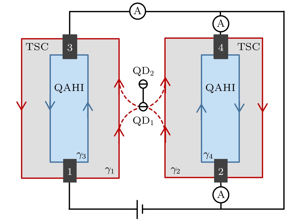
We study the resonance exchanges of two chiral Majorana fermions in two distinct systems theoretically in this work: one is an isolated Majorana zero mode interacting with complexes formed by two chiral Majorana fermions and a Majorana zero mode, and the other involves isolated quantum dots that are coupled to a system composed of Majorana fermions and a quantum dot. Our research results reveal that both of these coupled systems can facilitate the effective transmissions of the two chiral Majorana fermions as
$ {\gamma _1} \to - {\gamma _2} $
and
$ {\gamma _2} \to - {\gamma _1} $
, and the resonant tunneling effects in the two systems are equivalent. Therefore, quantum dots can replace Majorana zero modes to achieve resonant tunneling. In order to observe the resonance exchange of two chiral Majorana fermions with the two quantum dots, a circuit based on anomalous quantum Hall insulator proximity-coupled with s-wave superconductor is proposed as shown in figure. The numerical results indicate that the resonant exchange of chiral Majorana fermions can be modulated by the coupling strength between the two quantum dots, and it is particularly noteworthy that the tunneling process is independent of the superconducting phase. If one of the chiral Majorana fermions undergoes resonance coupling with another quantum dot or Majorana zero mode, an additional negative sign is obtained, leading to
$ - {\gamma _2} \to {\gamma _1} $
. After experiencing two resonance exchange processes, the final result is
$ {\gamma _1} \to {\gamma _2} $
and
$ {\gamma _2} \to - {\gamma _1} $
, which implies the realization of non-Abelian braiding operations. Our conclusion is that the modulation of coupling strength between two quantum dots can be used to achieve the switch of Majorana fermions braiding-like operation, which is independent of superconducting phase. Therefore, the designed scheme provides a new way for adjusting the braiding-like operation of Majorana fermions. These findings may have potential applications in the realization of topological quantum computers.


EDITOR'S SUGGESTION
2024, 73 (13): 130503.
doi:10.7498/aps.73.20240376
Abstract +
The quantum system composed of optical lattice and ultracold atomic gas is an ideal platform for realizing quantum simulation and quantum computing. Especially for dipolar bosons in optical lattices with artificial gauge fields, the interplay between anisotropic dipolar interactions and artificial gauge fields leads to many novel phases. Exploring the phase transition characteristics of the system is beneficial to understanding the physics of quantum many-body systems and observing quantum states of dipolar system in experiments. In this work, we investigate the quantum phase transitions of anisotropic dipolar bosons in a two-dimensional optical lattice with an artificial magnetic field. Using an inhomogeneous mean-field method and a Landau phase transition theory, we obtain complete phase diagrams and analytical expressions for phase boundaries between an incompressible phase and a compressible phase. Our results show that both the artificial magnetic field and the anisotropic dipolar interaction have a significant effect on the phase diagram. When the polar angle increases, the system undergoes the phase transition from a checkerboard supersolid to a striped supersolid. For small polar angle (
$V_x/U= 0.2, V_y/U=0.1$
, Fig.(a)), artificial magnetic field induces both checkerboard solid phase and supersolid phase to extend to a large hopping region. For a larger polar angle (
$V_x/U=0.2, $
$ V_y/U=-0.1$
, Fig.(b)), artificial magnetic field induces both striped solid and striped supersolid to extend to a large hopping region. Thus, the artificial magnetic field stabilizes the density wave and supersolid phases. In addition, we reveal the coexistence of different quantum phases in the presence of an external trapping potential. The research results provide a theoretical basis for manipulating the quantum phase in experiments on anisotropic dipolar atoms by using an artificial magnetic field.


2024, 73 (13): 130701.
doi:10.7498/aps.73.20240397
Abstract +
The atomic polarizability represents the response characteristics of atoms to externally applied electro-magnetic fields. The wavelength (or frequency) at which the dynamic polarizability of an atom is equal to zero is referred to as the tune-out wavelength (or frequency). Spectroscopy technology based on the tune-out effect has potential applications in quantum precision measurement, quantum computation and quantum communication. Related research topics include the measurement of fundamental physical constants and strong interactions. The tune-out wavelengths of atoms in low-lying states primarily fall within the optical band, where the theoretical calculations and experimental measurements have significant progress. However, for Rydberg atoms in highly excited states, theoretical calculations are challenging due to their high density of atomic states. The difficulty of experimental measurement arises from small splitting of adjacent atomic energy levels. In this paper, we demonstrate the tune-out wavelengths measurement for Rydberg atoms in a cesium vapor cell at room temperature. We utilize a two-photon cascade excitation to prepare Rydberg states and employ amplitude-modulation electromagnetically-induced transparency (AM-EIT) spectroscopy to measure the tune-out wavelength. By continuously scanning the microwave frequencies, we obtain AM-EIT signals of Rydberg atoms. At near-resonant microwave transition wavelengths, strong AM-EIT signals are observed due to microwave-atom coupling. Conversely, at tune-out wavelengths, the dynamically polarization-induced destructive interference in neighboring energy states occurs which leads to the weak AM-EIT signals. The AM-EIT provides a spectral resolution of about 10 MHz. We have developed a simplified three-level model to calculate the tune-out wavelength. The results of our theoretical calculations are consistent with the experimental findings within a range of ±90 MHz.
THE PHYSICS OF ELEMENTARY PARTICLES AND FIELDS

2024, 73 (13): 131401.
doi:10.7498/aps.73.20240447
Abstract +


NUCLEAR PHYSICS
2024, 73 (13): 132301.
doi:10.7498/aps.73.20240276
Abstract +


SPECIAL TOPIC—Modification of material properties by defects and dopants
EDITOR'S SUGGESTION
2024, 73 (13): 137802.
doi:10.7498/aps.73.20240475
Abstract +
ATOMIC AND MOLECULAR PHYSICS
2024, 73 (13): 133101.
doi:10.7498/aps.73.20240417
Abstract +
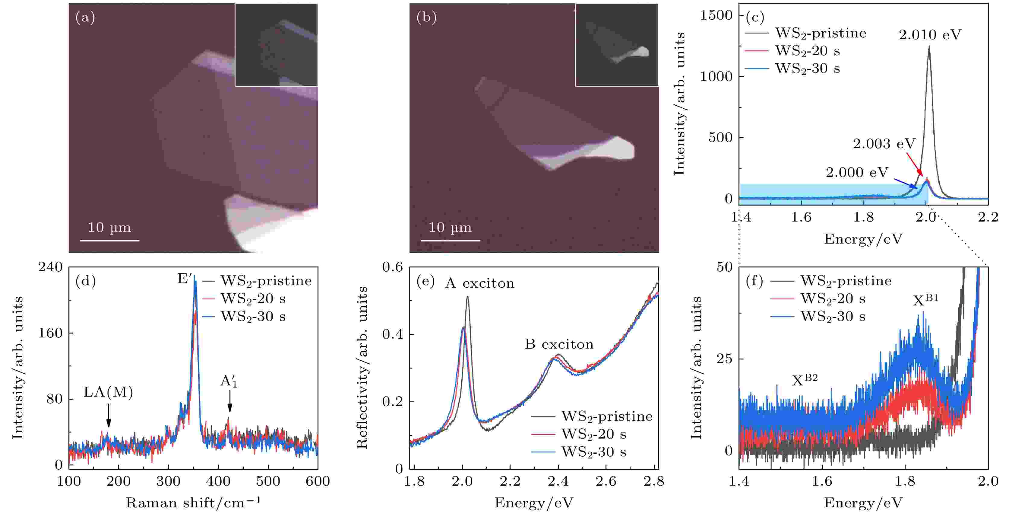
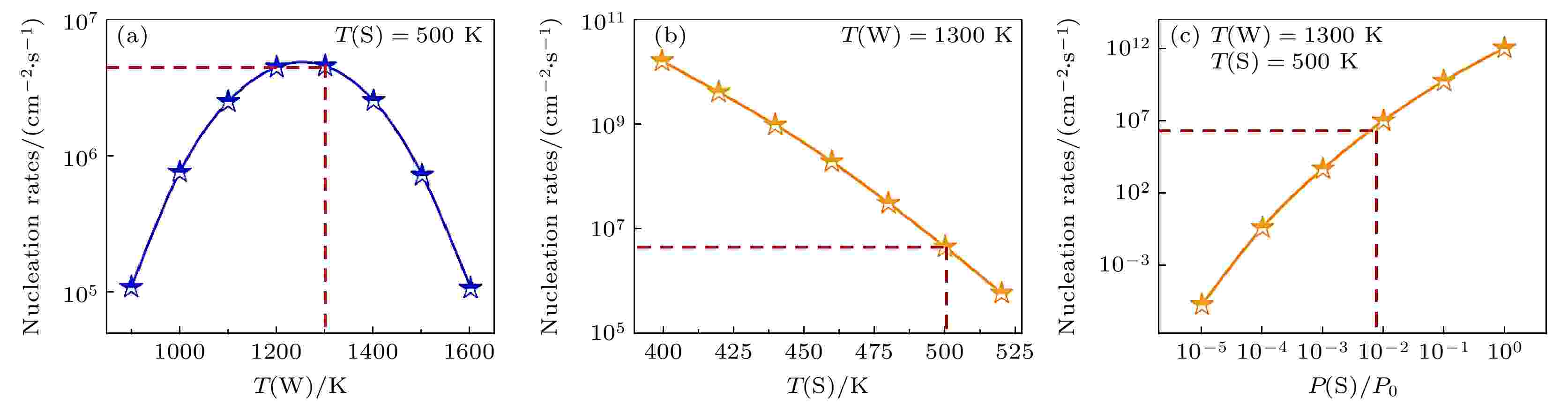
Two-dimensional tungsten disulfide (WS2), as a semiconductor material with unique layer-dependent electronic and optoelectronic characteristics, demonstrates a promising application prospect in the field of optoelectronic devices. The fabrication of wafer-scale monolayer WS2films is currently a critical challenge that propels their application in advanced transistors and integrated circuits. Chemical vapor deposition (CVD) is a feasible technique for fabricating large-area, high-quality monolayer WS2films, yet the complexity of its growth process results in low growth efficiency and inconsistent film quality of WS2. In order to guide experimental efforts to diminish grain boundaries in WS2, thereby improving film quality to enhance electronic performance and mechanical stability, this study investigates the nucleation mechanisms of WS2during CVD growth through first-principles theoretical calculations. By considering chemical potential as a crucial variable, we analyze the growth energy curves of WS2under diverse experimental conditions. Our findings demonstrate that modulating the temperature or pressure of the tungsten and sulfur precursors can decisively influence the nucleation rate of WS2. Notably, the nucleation rate reaches a peak at a tungsten source temperature of 1250 K, while an increase in sulfur source temperature or a decrease in pressure can suppress the nucleation rate, thereby enhancing the crystallinity and uniformity of monolayer WS2. These insights not only furnish a robust theoretical foundation for experimentally fine-tuning the nucleation rate as needed but also provide strategic guidance for optimizing experimental parameters to refine the crystallinity and uniformity of monolayer WS2films. Such advancements are expected to accelerate the deployment of WS2materials in a range of high-performance electronic devices, marking a significant stride in the field of materials science and industrial applications.
ELECTROMAGNETISM, OPTICS, ACOUSTICS, HEAT TRANSFER, CLASSICAL MECHANICS, AND FLUID DYNAMICS
2024, 73 (13): 134201.
doi:10.7498/aps.73.20240269
Abstract +
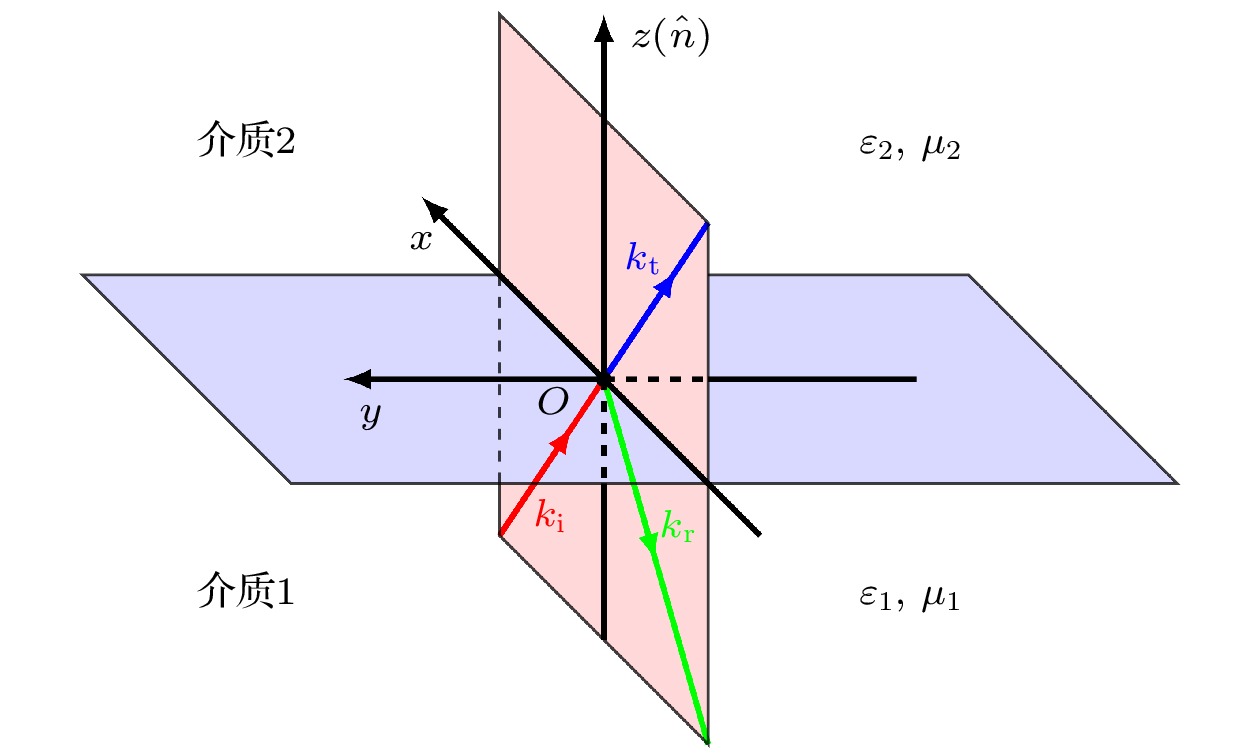
Due to the boundary conditions of electromagnetic fields and phase matching of electro magnetic waves on interface being the basis to drive the Snell’s laws and Fresnel’s laws, they are also crucial for the analysis of electromagnetic wave propagation in a moving medium. There are mainly two methods to derive the boundary conditions of electromagnetic fields on moving interface. One of them is to use the kinematic integral form, yet this method is based on the classical time-space, and the other is based on the relativistic transformation, the boundary conditions are derived from the scaling effect with geometric method, or from the principle of relativity directly. However, the first one has a form the same as the form obtained by using the kinematic integral form, while the second one obtains a different form. At the same time, the phase matching of electromagnetic wave on moving interface is only discussed by Galileo transformation, however this is unreasonable, because of the relativistic effect cannot be ignored here. Therefore, it is necessary to reexamine the boundary conditions of electromagnetic fields and phase matching of electromagnetic wave on moving interface. Herein, firstly, the relativistic transformation formula of the unit normal vector of moving surface is derived from the surface equation and principle of relativity. Secondly, the boundary conditions of electromagnetic fields on moving interface are given based on the relativistic transformation formula and the non-relativistic transformation formula of the unit normal vector and electromagnetic fields, which show that the boundary conditions of electromagnetic fields on moving interface under the relativistic case and the non-relativistic case have the same form. This is not accidental but definite, because the change of flux of electromagnetic fields, like the change of magnetic flux, from the induction of electromagnetic filed is the same as that from the variation of surface element. Thirdly, the phase matching of electromagnetic wave on moving interface is given based on the relativistic transformation formula of the unit normal vector and the phase matching of electromagnetic wave on resting interface. In the problem of light incident on a homogeneous medium moving at a constant velocity in vacuum or air, using the phase matching of electromagnetic wave on moving interface, the same results can be easily obtained through other methods. The discussion in this study belongs to classical electrodynamics with no quantum effects considered, but the results will provide some conveniences for theoretically analyzing electromagnetic communication, remote sensing and telemetering.
2024, 73 (13): 134202.
doi:10.7498/aps.73.20231652
Abstract +
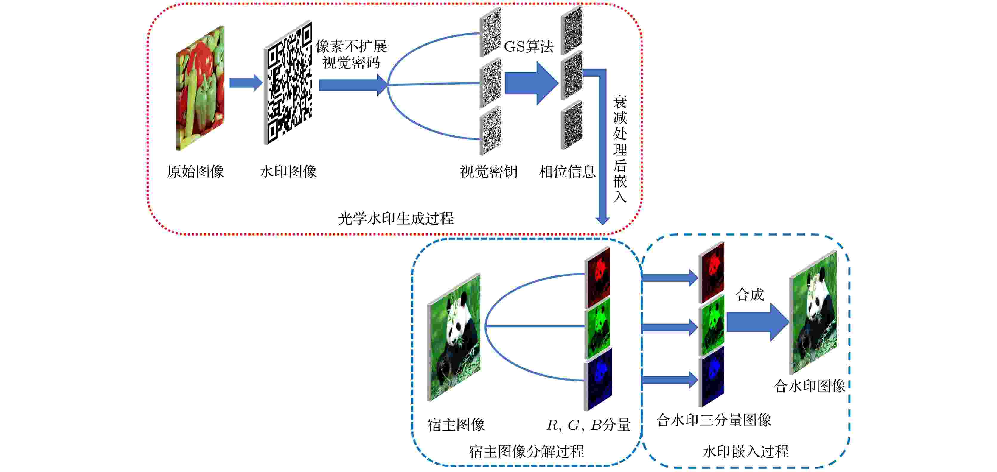
In recent years, with the continuous development of computer technology, it has brought convenience to people to obtain image information. However, at the same time, the falsification and theft of image information have also emerged, so information security has received increasing attention. When images are used for medicine, military, court, and other purposes, it is necessary to ensure the authenticity and integrity of the image content. Fragile watermarks are used to verify the authenticity and integrity of image content due to their sensitivity to tampering. The watermark information is embedded in the image and integrated with the image. When it is necessary to detect the authenticity and integrity of image information, the extracted watermark can be used to determine whether the image is reliable and complete. Therefore, we propose an optical color fragile watermarking system based on pixel-free expansion visual cryptography. On the one hand, encoding watermark images by using pixel-free expansion visual cryptography avoids pixel expansion issues caused by visual cryptography, allowing for the selection of color host images with the same pixel size as the watermark image in the future, greatly reducing the network bandwidth and storage space occupied during transmission. On the other hand, phase recovery algorithm is used to process the encoded watermark image to obtain phase information for embedding into the host image, further improving the security of the watermark image in an optical way. The feasibility and imperceptibility of the proposed optical color fragile watermark are verified through computer simulation, and its good fragility is verified through a series of simulation attack experiments. It can sensitively detect image tampering in the face of common attacks such as noise pollution, rotation, motion blur processing, filtering, etc.
2024, 73 (13): 134203.
doi:10.7498/aps.73.20240407
Abstract +
The intensity-difference squeezed state is an important concept in quantum optics, which is not only of great significance for fundamental research in quantum physics, but also an important quantum resource in the fields of quantum communication, quantum computing, and quantum precision measurement. The optical parametric amplifier based on atomic four-wave mixing is one of the most effective means to achieve intensity-difference squeezed light. However, due to the absorption loss of atomic vapor in the light field, the output squeezing still needs improving. By feeding the non-classical optical field from the optical parametric amplifier back to the input port, the quantum characteristics of its output optical field can be enhanced. However, the intensity-difference squeezing enhancement from a phase-insensitive amplifier is experimentally realized based on coherent feedback control. The intensity-difference squeezing enhancement of the phase-sensitive amplifier has not been discussed. In this work, a two-port coherent feedback-controlled phase-sensitive amplifier is analyzed theoretically. The dependence of the intensity-difference squeezing, respectively, on the feedback intensity, the intensity gain of the optical parametric amplifier, and the losses of the system are investigated. For the ideal case in which the losses of the system are ignored, infinite squeezing can be achieved by adjusting the strength and phase of feedback. Considering the actual atomic absorption losses, squeezing enhancement can also be achieved over a wide range of intensity gains within a certain feedback intensity range. In addition, the squeezing enhancement is quite efficient for the medium intensity gain range. The intensity-difference squeezing enhancement strongly depends on the absorption loss of atomic vapor. The smaller the absorption loss, the more significant the squeezing enhancement effect is. Furthermore, the experimental feasibility of this scheme is also considered in detail. Our research can provide useful references for achieving high-quality non classical light fields in experiment, which may find applications in quantum information processing and quantum precise measurement.
EDITOR'S SUGGESTION
2024, 73 (13): 134204.
doi:10.7498/aps.73.20240300
Abstract +
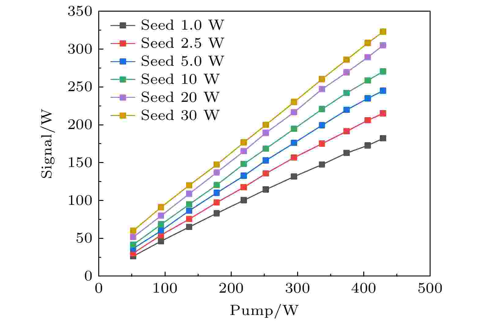
Ytterbium-doped ultrafast fiber lasers are widely used in scientific research, industrial processing, medical diagnosis, and other fields due to their excellent beam quality and high power output. The larger mode area allows the fiber to transmit higher peak-pulse power. The commercial rod-type Ytterbium-doped fiber with a core diameter of 85 μm, produced by NKT in Denmark, can produce ultra-short pulses on the order of 100 watts and 100 microjoules. Based on this rod-type fiber, we construct a chirped-pulse amplification (CPA) system in which the high-efficiency transmission gratings and temperature-tunable chirped fiber Bragg grating (CFBG) are used to compensate for dispersion. We investigate the effect of power input on the amplified power and pulse compression quality, and find that higher power input slows down the gain saturation and improves amplification efficiency. At power inputs of 20 W and 30 W, we obtain power outputs of 305 W and 323 W respectively, with an amplification efficiency of about 80%. To reduce the accumulation of nonlinear phase shift, we use circular polarization amplification. At low power outputs (less than 160 W), the effect of nonlinear phase accumulation on the compressed pulse is negligible, and the increase in power input increases the amplification efficiency. When the power output exceeds 200 W, the cumulative increase of nonlinear phase shift reduces the pulse compression quality, which implies that the input power is appropriately reduced to the power range between 5 W and 20 W. With a power input of 20 W and pump power of 429 W, the power output can reach 305 W. After pulse is compressed by using a diffraction-grating pair, this rod-type fiber CPA system can deliver 1 MHz, 264 fs pulses with 273 W in average power. These results provide an important experimental basis for optimizing the performance of high-power and high-energy ultrafast fiber lasers.

EDITOR'S SUGGESTION
2024, 73 (13): 134205.
doi:10.7498/aps.73.20240427
Abstract +
The Hermite-Gaussian (HG) beam has many potential advanced applications in optical communications, electron acceleration, nonlinear optics and bio-optical disease detection, owing to its distinctive mode and intensity distribution. The research on HG beam are significant in the development of optics, medicine and quantum technology. However, the controlling of the evolutions of HG beam with quadratic phase modulation (QPM) in fractional systems under variable coefficients and potentials has been rarely studied. In this work, the propagation dynamic behaviors of the HG beam with QPM are investigated based on the fractional Schrödinger equation (FSE) under different variable coefficients and potentials by using a split-step Fourier algorithm. In the free space, the focusing spot of the beam becomes larger as the positive QPM coefficient increases or the Lévy index decreases. The QPM coefficient has little effect on the focusing amplitude when the Lévy index is 2. When the QPM coefficient is negative, the focusing of the beam disappears. Under the joint action of cosine modulations and QPM, the transmission of the beam oscillates not by the cosine law, but presents a large and a small breathing structure. The positive and the negative coefficient of QPM only alter the breathing sequence. The evolution period and width of the beam decrease as the modulation frequency increases. The trajectory of split beams turns into a parabolic shape under the linear modulation. In the joint influence of linear modulations and QPM, the HG beam exhibits either focusing or not focusing. Furthermore, the focusing position and focal plane of the beam decrease as the Lévy index increases. When the Lévy index is small, the beam keeps a straight-line transmission without distortion at a longer distance under the joint effect of the power function modulation and a positive QPM. The transmission of the beam also stabilizes and the beam width becomes larger with a negative QPM. Under a linear potential, the splitting of the HG beam disappears with the increase of the linear coefficient and shows a periodic evolution. The propagation trajectory of the beam shows a serrated pattern. By adding QPM, the beam is significantly amplified. Additionally, the evolution period of the beam is inversely proportional to the linear coefficient, and the transverse amplitude turns larger as the Lévy index increases. The interference among beams is strong, but it also exhibits an autofocus-defocusing effect under the joint action of a parabolic potential and QPM. In addition, the positive coefficient and the negative coefficient of QPM only affect the focusing time of the beam. The frequency of focusing increases as the Lévy index and parabolic coefficient rise. These features are important for applications in optical manipulations and optical focusing.
2024, 73 (13): 134206.
doi:10.7498/aps.73.20240288
Abstract +
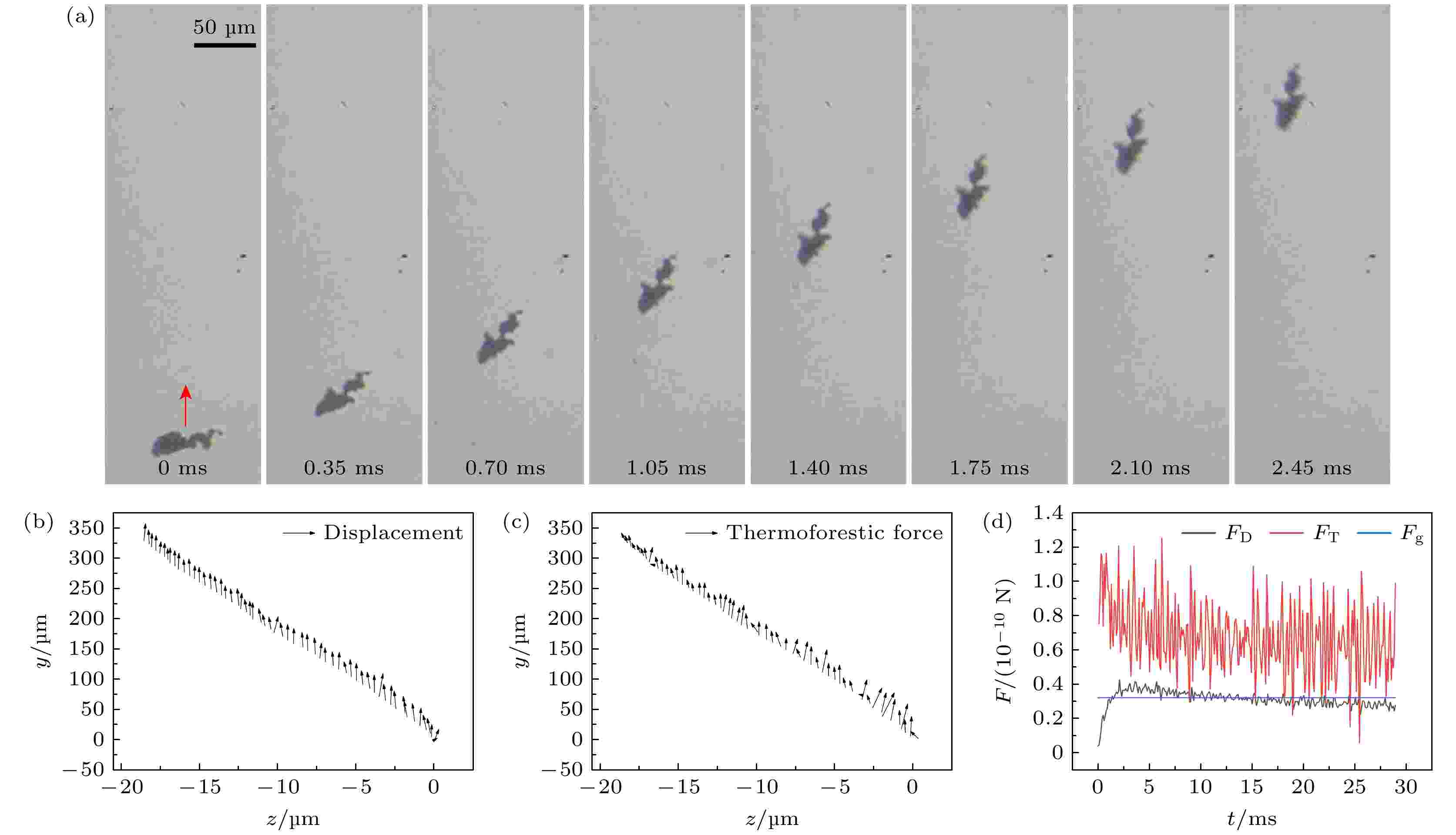
In order to explore the levitation and migration behavior of strongly absorbing nanoparticle clusters in air by using laser technique, in this study trapping and levitating nanoparticle clusters is proposed based on the counter-propagated bi-Bessel beams, and then the clusters are released to observe and analyze their migration behaviors. Two Bessel beams are generated by a conical lens and polarizing beam splitter, arranged horizontally in reverse to form a three-dimensional optical trap. The stiffness of the optical trap can be controlled by adjusting the power ratio of the two Bessel beams. The particles in the levitation chamber are fluidized through weak airflow, and then captured and levitated by a light trap. A high-speed camera is used to record the levitation and migration process of clusters. The particle motion parameters can be obtained through image analysis. The strong-absorbing ultrafine coal particle clusters are first selected to conduct the experiments on their levitation and release migration. Then, the photophorestic force, gravity, buoyancy, drag force, and thermophorestic force acting on the clusters are calculated and analyzed. The experimental and computational results indicate that the photophorestic force of air-borne strong-absorbing nanoparticle clusters generated by laser illumination dominates the levitation; nanoparticle clusters can be stably levitated in a three-dimensional potential well formed by counter-propagated bi-Bessel beams, achieving dynamic equilibrium with gravity, buoyancy, drag, etc. by adjusting the levitation position. The relative instability parameter of levitation is used to evaluate the stability of air-borne strong-absorbing nanoparticle clusters, and the minimum relative instability of ultrafine coal particle clusters reaches 0.075. By analyzing the images of nanoparticle cluster recorded by high-speed camera after being released, the migration motion parameters of the cluster can be obtained, therefore the thermophorestic force acting on the cluster is accurately measured. For the ultrafine coal particle clusters with equivalent particle sizes in a range of approximately 13–21 μm, the magnitudes of their thermophorestic forces are in a range of 10–11–10–10N. As the cluster size increases, the thermophorestic force increases linearly, which is consistent with the theoretical calculation trend. The use of laser to levitate and release particles provides a novel approach for measuring and analyzing thermophorestic force, and also presents a novel manipulation tool for controlling and transporting particles in a gaseous medium.
2024, 73 (13): 134301.
doi:10.7498/aps.73.20231911
Abstract +
The difference in intensity fluctuation between a surface signal and a submerged signal can be used to discriminate the source depth in the shallow water waveguide. However, the properties of fluctuation distinction in intensity between surface source and submerge source are rarely studied, resulting in the poor performance of fluctuation-based methods sometimes. In this work, the intensity fluctuations caused by source depth fluctuations is analyzed by differential method and variance statistics method to figure out the physics of intensity fluctuations, and to present the suitable quantity for depth discrimination. Firstly, the derivative expression of real part, power and amplitude of the pressure field are respectively derived from the normal mode theory, hence their fluctuation quantities are specified. Then, the numerical examples, including the factor of receiver depth, source frequency and source range, are treated to verify the derivation and summarize the characteristic of fluctuations. The property of the intensity fluctuations is also compared with the distribution of normalized quantity on the depth dimension. Finally, the SWellEx-96 experimental data processing results validate the conclusions. The processing results of derivation, simulation data and experimental data show that the interactions between modes excited by the source give rise to the fluctuations. Meanwhile, the property of the interactions is affected by the received depth, source range and source frequency. Amplitude is capable of building a quantity based on fluctuations for source depth discrimination. For surface and submerged sources with lower frequency, their distinction in their fluctuations is stably represented by amplitude. In the SWellEx-96 experiment, the normalized values calculated from the amplitude of surface noise and submerged sound sources show the lowest difference of 0.5 and the highest difference of 2.5, indicating the effectiveness of using amplitude fluctuations to discriminate the sound source depth.

2024, 73 (13): 134701.
doi:10.7498/aps.73.20240394
Abstract +
Bubble motion in non-Newtonian fluids is widely present in various industrial processes such as crude oil extraction, enhancement of boiling heat transfer, CO2sequestration and wastewater treatment. System containing non-Newtonian liquid, as opposed to Newtonian liquid, has shear-dependent viscosity, which can change the hydrodynamic characteristics of the bubbles, such as their size, deformation, instability, terminal velocity, and shear rate, and ultimately affect the bubble rising behaviors. In this work, the dynamic behavior of bubble rising in a shear-thickened fluid is studied by using an incompressible lattice Boltzmann non-Newtonian gas-liquid two-phase flow model. The effects of the rheological exponentn, the Eötvös number (Eo), and the Galilei number (Ga) on the bubble deformation, terminal velocity, and the shear rate are investigated. The numerical results show that the degree of bubble deformation increases asEogrows, and the effect ofnon bubble deformation degree relates toGa. On the other hand, the terminal velocity of the bubbles increases monotonically and nonlinearly withGafor givenEoandn, and the effect ofnon the terminal velocity of the bubbles turns stronger asGaincreases. WhenGais fixed and small, the terminal velocity of the bubble increases and then decreases with the increase ofnat smallEo, and increases with the increase ofnwhenEois large; but whenGais fixed and large, the terminal velocity of the bubbles increases with the increase ofnin a more uniform manner. In addition, regions with high shear rates can be found near the left end and right end of the bubble. The size of these regions grows withEoandGa, exhibiting an initial increase followed by a decrease asnincreases. Finally, the orthogonal experimental method is used to obtain the influences of the aforementioned three factors on the shear rate and terminal velocity. The order of influence on shear rate isn,GaandEowhich are arranged in descending order. For the terminal velocity,Gahas the greatest influence, followed byn, andEohas the least influence.

EDITOR'S SUGGESTION
2024, 73 (13): 134702.
doi:10.7498/aps.73.20240399
Abstract +
To investigate the hydrodynamic performance of manta rays swimming in staggered arranged group, a morphological and kinematic model of manta rays is developed based on biological observations, and then a numerical calculation method is established for group swimming of manta rays based on the Immersed Boundary Method and the Sphere function-based Gas Kinetic Scheme (IB-SGKS). The group swimming of two manta rays with a fixed vertical spacing of 0.1 times the body thickness, and a flow direction spacing of 0—1.5 times the body length is systematically investigated. The average thrust/efficiency of the group system and each individual in the group are analyzed by combining the global three-dimensional (3D) vortex structure and the characteristic cross-section two-dimensional (2D) vortex structure. The numerical results are shown below. When the streamwise spacing between individuals is small, the propulsive performance decreases sharply compared with swimming alone; as the streamwise spacing increases, the propulsive performance of the leader manta ray is consistently better than that of swimming alone, with the maximum thrust enhanced up to 11.24% whenDx= 0.4BL, and the maximum efficiency is enhanced up to 3.58% whenDx= 0.3BL; with the increase of the streamwise spacing, in the thrust/efficiency curves of the follower manta ray appears volatility, with the maximum thrust enhanced to 48.14% whenDx= 0.4BL and the maximum efficiency reached to 12.39% whenDx= 0.5BL; the system average thrust and efficiency enhancement both reach their corresponding maximum values, specifically, 29.69% and 6.77%, whenDx= 0.4BL, which is because the tail vortex of the leading manta ray just passes through the front edge of the follower manta ray and directly acts on the tip vortex that initially falls off from the follower manta rays, thus substantially increasing their vortex energy.
PHYSICS OF GASES, PLASMAS, AND ELECTRIC DISCHARGES
2024, 73 (13): 135201.
doi:10.7498/aps.73.20240436
Abstract +
In the inductively coupled plasma (ICP) discharge, surface processes, such as reflection, de-excitation, and recombination, can occur when active species arrive at material surfaces, which accordingly influences the plasma properties. In this work, a fluid model is used to study the Ar/O2plasma generated by ICP reactors made of different materials. In simulation, sticking coefficient is employed to estimate the surface reactions on different materials. As the reactor material changes from stainless steel to anodized aluminum to Cu, the sticking coefficient of surface reaction O→1/2O2decreases accordingly. It is found that the reactor material has a great effect on species density. In the stainless steel reactor, the density of O atoms at grounded state and excited state are much lower because more O2molecules are generated from the surface reaction, yielding a much higher density of
$ {\text{O}}_2^ + $
molecular ions which are mainly created from the ionization process of O2molecules. Similarly, the high density of O2molecules also enhances the production of
${{{\mathrm{O}}} _2}\left( {{{\mathrm{a}}^1}{\Delta _{\mathrm{g}}}} \right)$
molecules through the excitation process and O–ions through the dissociation attachment reaction. On the contrary, more electrons are consumed via the collisions between electrons and O2molecules or
$ {\text{O}}_2^ + $
molecular ions. Therefore, the electron density obtained in the Cu reactor is highest. The density of Ar+ions and Armatoms also increase with sticking coefficient decreasing. The density of O+ions and
$ {\text{O}}_2^ + $
molecular ions peak below the coil in the stainless steel reactor, whereas the radial uniformities are improved in the Cu reactor. In the three reactors, the electrons distribute evenly at the reactor center region. The O density and
${{{\mathrm{O}}} _2}\left( {{{\mathrm{a}}^1}{\Delta _{\mathrm{g}}}} \right)$
density significantly peak at the reactor center, while the maximum value of Ar+density and Armdensity are below the coil. As for O(1D), the maximum density below the coil region moves toward the reactor center as the reactor material changes from stainless steel to Cu. Finally, the effect of sticking coefficient of O→1/2O2is studied. The results show that the O atom density decreases with the sticking coefficient increasing, but the opposite trend is observed in O2molecular density. It is noticed that the sticking coefficient has little effect on species density when it is higher than 0.5.


EDITOR'S SUGGESTION
2024, 73 (13): 135202.
doi:10.7498/aps.73.20240497
Abstract +

CONDENSED MATTER: ELECTRONIC STRUCTURE, ELECTRICAL, MAGNETIC, AND OPTICAL PROPERTIES
EDITOR'S SUGGESTION
2024, 73 (13): 137101.
doi:10.7498/aps.73.20240434
Abstract +
Two-dimensional semiconductor heterostructures have excellent physical properties such as high light absorption coefficients, large diffusion lengths, high carrier mobility rates, and tunable energy band structures, which have great potential in the field of optoelectronic devices. Therefore, designing two-dimensional (2D) semiconductor van der Waals heterostructures is an effective strategy for realizing multifunctional microelectronic devices. In this work, the 2D van der Waals heterostructure Cs3X2I9/InSe of non-lead Perovskite Cs3X2I9and indium-tin InSe is constructed to avoid the toxicity and stability problems of lead-based Perovskites. The geometry, electronic structure, and optical properties are calculated based on the first-principles approach of density-functional theory. It is shown that the 2D Cs3Bi2I9/InSe and Cs3Sb2I9/InSe heterostructures are of type-II energy band arrangement and have band gaps of 1.61 eV and 1.19 eV, respectively, with high absorption coefficients in the visible range and UV range reaching to 5×105cm–1. The calculation results from the deformation potential theory and the hydrogen-like atom model show that the 2D Cs3X2I9/InSe heterostructure has a high exciton binding energy (~0.7 eV) and electron mobility rate (~700 cm2/(V·s)). The higher light absorption coefficient, carrier mobility, and exciton energy make the 2D Cs3X2I9/InSe heterostructures suitable for photoluminescent devices. However, the energy band structure based on the Shockley-Queisser limit and type-II arrangement shows that the intrinsic photoelectric conversion efficiency (PCE) of the 2D Cs3X2I9/InSe heterostructure is only about 1.4%, which is not suitable for photovoltaic solar energy. In addition, the modulation and its effect of biaxial strain on the photovoltaic properties of 2D Cs3X2I9/InSe heterostructures are further investigated. The results show that biaxial strain can improve the visible absorption coefficient of 2D Cs3X2I9/InSe heterostructure, but cannot effectively improve its energy band structure, and the PCE only increases to 3.3% at –5% biaxial strain. The above study provides a theoretical basis for designing efficient 2D van der Waals optoelectronic devices in future.
2024, 73 (13): 137102.
doi:10.7498/aps.73.20240530
Abstract +
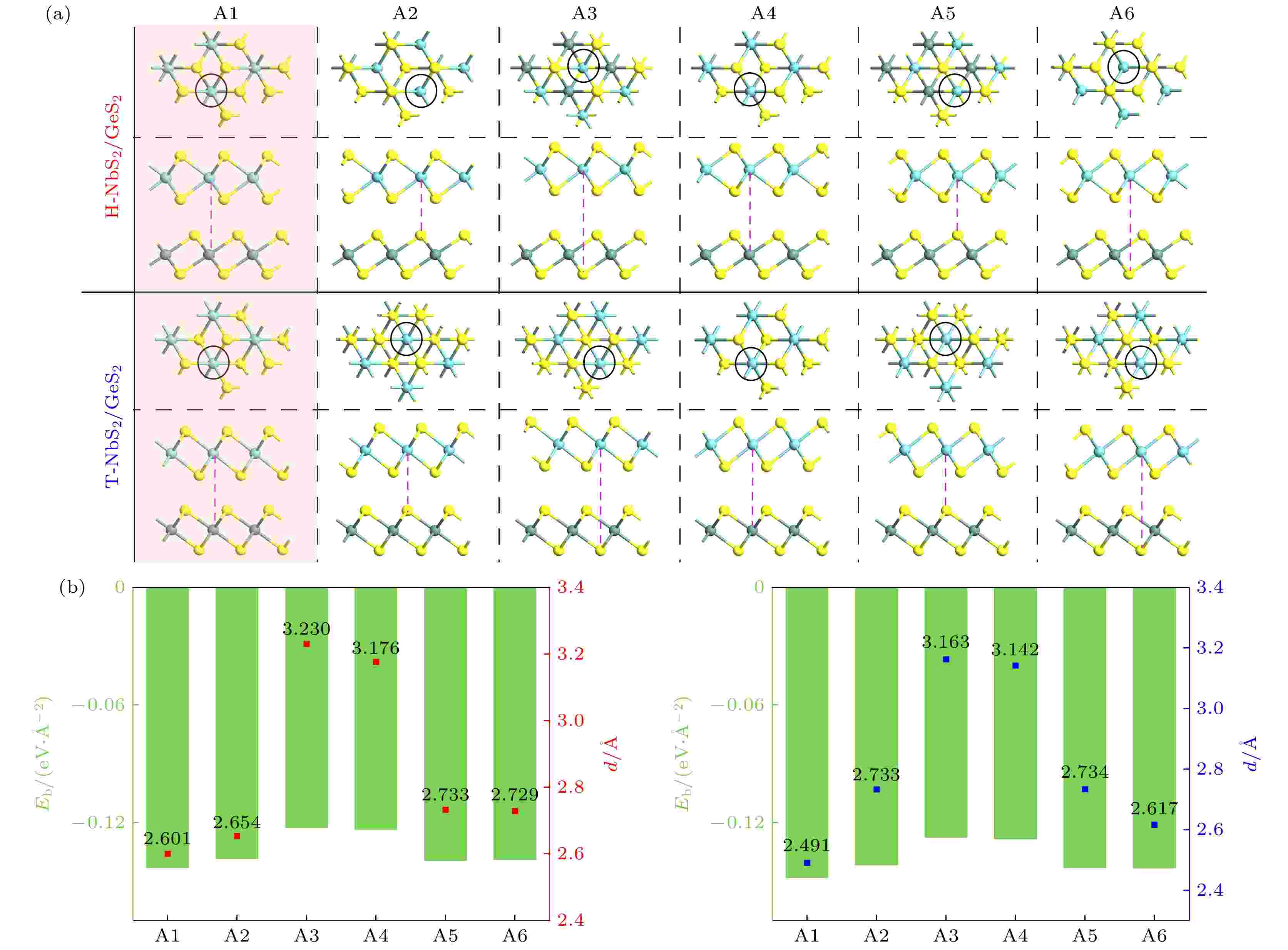
Metal-semiconductor heterojunction (MSJ) is the basis for developing novel devices. Here, we consider different two-dimensional van der Waals MSJs consisting of different-phase metals H- and T-NbS2and semiconductor GeS2, and conduct an in-depth study of their structural stabilities, electronic and electrical contact properties, with an emphasis on exploring the dependence of the electrical contact properties of the MSJs on the different phases of metals. Calculation results of their binding energy, phonon spectra, AIMD simulations, and mechanical properties show that both heterojunctions are highly stable, which implies that it is possible to prepare them experimentally and feasible to use them for designing electronic devices. The intrinsic H-NbS2/GeS2and T-NbS2/GeS2heterojunctions form p-type Schottky contacts and quasi-n-type Ohmic contacts, respectively. It is also found that their Schottky barrier heights (SBHs) and electrical contact types can be effectively modulated by an applied electric field and biaxial strain. For example, for the H-NbS2/GeS2heterojunction, Ohmic contact can be achieved regardless of applying a positive/negative electric field or planar biaxial compression, while for the T-NbS2/GeS2heterojunction, Ohmic contact can be achieved only at a very low negative electric field. The planar biaxial stretching can achieve quasi-Ohmic contact. In other words, when the semiconductor GeS2monolayer is used as the channel material of the field effect transistor and contacts different metal NbS2monolayers to form the MSJ, the interfacial Schottky barriers are distinctly different, and each of them has its own advantages in different situations (intrinsic or physically regulated). Therefore, this study is of great significance for understanding the physical mechanism of the electrical contact behaviors for H(T)-NbS2/GeS2heterojunction, especially for providing the theoretical reference for selecting suitable metal electrodes for the development of high-performance electronic devices.
2024, 73 (13): 137103.
doi:10.7498/aps.73.20231979
Abstract +
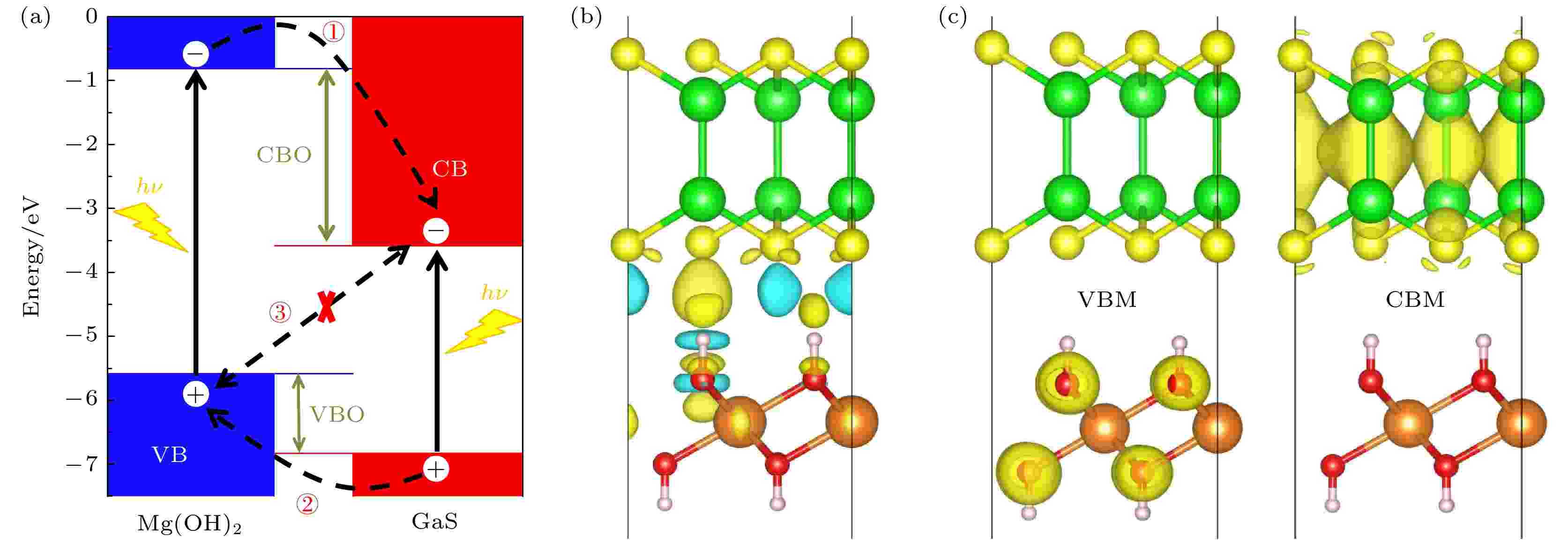
Constructing Type-II heterostructure is an effective scheme to tailor the electronic structure and improve the application performance. Motivated by recently successful syntheses of Mg(OH)2and GaS monolayers, we investigate the stability, electronic, and optical properties of GaS/Mg(OH)2heterostructure by using the density functional theory method. The calculated results show that GaS/Mg(OH)2heterostructure is easily constructed due to its small lattice mismatch, negative binding energy, and thermodynamic stability. Compared with monolayer materials, the GaS/Mg(OH)2heterostructure has a band gap that effectively decreases to 2.021 eV and has Type-II band structure, facilitating the spatial separation of photo-generated carriers where electrons are localized in the GaS and holes reside in the Mg(OH)2monolayers. The built-in electric field induced by the interlayer charge transfer points from GaS to Mg(OH)2monolayer, which can further improve the separation and suppress the recombination of electron-hole pairs. Under the biaxial strain, the valance band maximum and conduction band minimum of GaS/Mg(OH)2heterostructure shift in the downward direction to different extents, resulting in obvious change of band gap, with the change reaching about 0.5 eV. Furthermore, the band structure of GaS/Mg(OH)2heterostructure can be transformed from indirect band gap semiconductor into direct band gap semiconductor under the tensile strain, while GaS/Mg(OH)2heterostructure maintains Type-II band structure. Additionally, the band edge positions of GaS/Mg(OH)2heterostructure can also be effectively adjusted to cross the redox potentials of water decomposition at pH = 0–7. The light absorption spectra show that GaS/Mg(OH)2heterostructure has stronger light absorption capability than the constituent monolayers. Especially, the light absorption has an obvious redshift phenomenon at a tensile strain of 3%. These findings indicate that the GaS/Mg(OH)2heterostructure has a wide range of applications in the field of optoelectronics due to the tunable electronic properties, and also provides some valuable insights for future research.
2024, 73 (13): 137201.
doi:10.7498/aps.73.20240510
Abstract +


Structural stability and electronic properties of charged point defects in monolayer blue phosphorus
2024, 73 (13): 137301.
doi:10.7498/aps.73.20240011
Abstract +
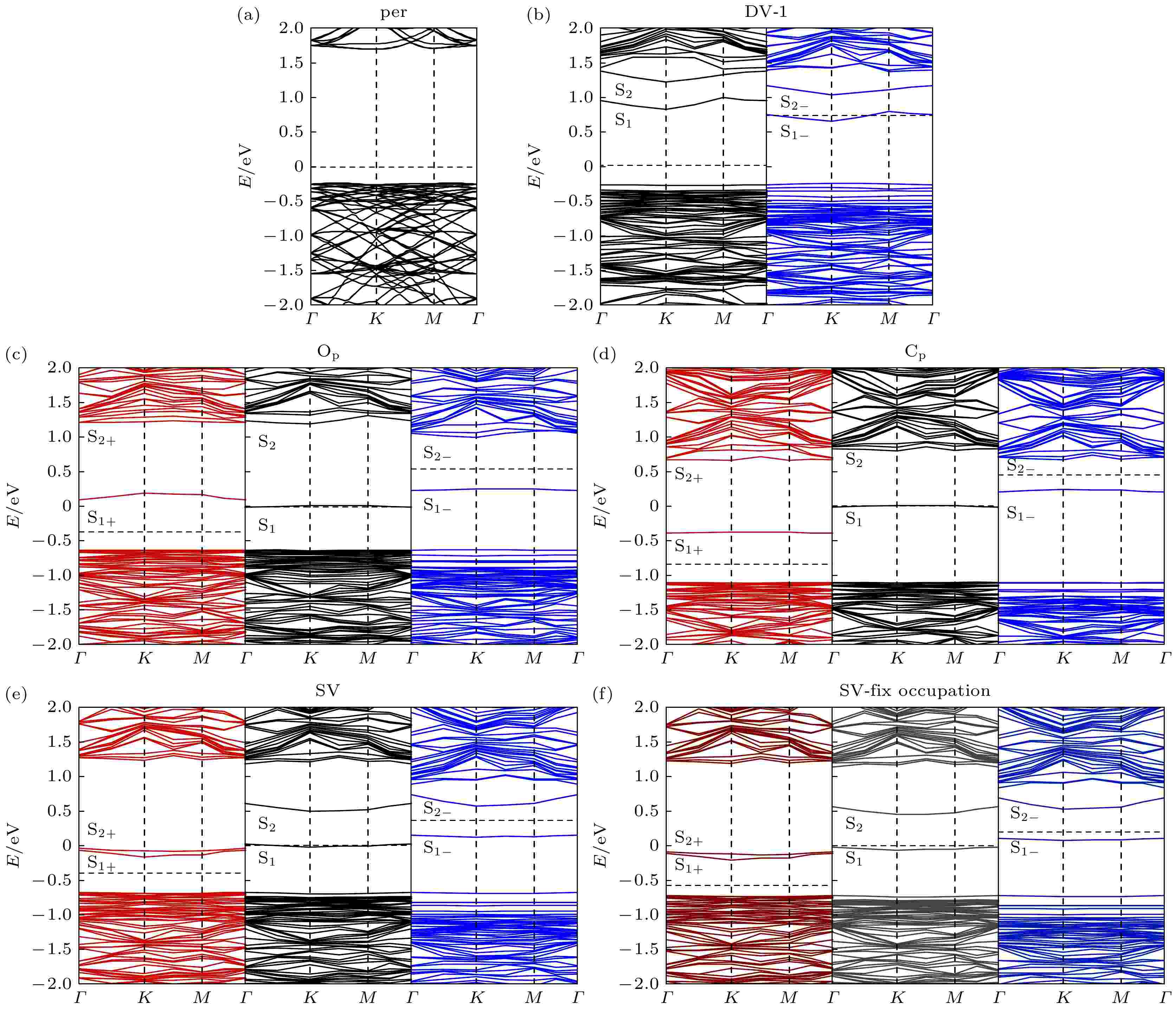
As a new two-dimensional material, blue phosphorus has attracted considerable research interest due to its high carrier mobility and large bandgap. Although the structural defects of blue phosphorus have been discussed recently, the charged properties of these defects have not been explored. In this paper, using first-principles calculations based on density functional theory, the six most stable point defects and their corresponding charged states in blue phosphorus are studied, including Stone Wales (SW), single vacancy (SV), two double-vacancy (DV-1 and DV-2) and two substitution defects (OPand CP). The converged ionization energy values of charged defects in blue phosphorus are obtained by extrapolating the asymptotic expression of the energy dependent on the cell size. Subsequently, the formation energy values for different charge states are modified to determine their structural stabilities. Finally, their electronic properties are analyzed through band structures. The results suggest that SV1–is easy to ionize, owing to its lowest ionization energy (1.08 eV). Furthermore, among the defects we are considering, OP1–is the most stable charged defect in blue phosphorus, with the lowest formation energy (–9.33 eV) under O-rich chemical potential condition. The negative formation energy indicates that O atoms can exist stably in blue phosphorus, implying that blue phosphorus is easily oxidized. The introduction of defect states will affect the bandgap of blue phosphorus, and the ionization of defects will cause the defect energy levels to shift, leading defects to transition between shallow and deep levels. This study provides theoretical guidance for the application of defect engineering in two-dimensional materials.

EDITOR'S SUGGESTION
2024, 73 (13): 137302.
doi:10.7498/aps.73.20240431
Abstract +

2024, 73 (13): 137501.
doi:10.7498/aps.73.20240437
Abstract +
Layered magnetic topological materials are material systems that exhibit both magnetic ordering and topological properties in their smallest two-dimensional units. Studying these systems may lead to the observation of new physical properties and phenomena, which has attracted considerable attention from researchers. The effect of interlayer exchange coupling interactions on bilayer honeycomb Heisenberg ferromagnets with interlayer coupled topological phase is investigated by using linear spin wave theory. The influence of introducing two additional types of interactions, i.e. interlayer exchange coupling interaction and interlayer easy-axis anisotropy interaction, on the topological phase transition are also explored in this work. By calculating the magnon dispersion relations at various interlayer exchange coupling interaction intensities, it is found that the band gaps of high energy band and low energy band both close and reopen at the Dirac points when the system reaches the critical value of interlayer exchange coupling interaction. In magnon systems, such physical phenomena typically relate to topological phase transitions. When calculating the Berry curvature and Chern numbers for the bands in the aforementioned process, it is found that the sign of the Berry curvature reverses and the Chern numbers change when the critical value of interlayer exchange coupling interaction strength is reached, confirming that a topological phase transition occurs indeed. Introducing two other types of interlayer exchange coupling interactions in this process can lead various novel topological phases to occur in the system. The enhancement of interlayer easy-axis anisotropy interactions is likely to impede the topological phase transitions occurring in the system. We find that a major distinction between bilayer honeycomb ferromagnets and their single-layer counterparts lies in the fact that during a topological phase transition, the sign of the magnon thermal Hall coefficient does not change; on the contrary, abrupt shift in the thermal Hall coefficient curve occurs which can be seen as an indicator of topological phase transition of bilayer honeycomb ferromagnets, and is also reflected in the change in magnon Nernst coefficient. The research results of this work can provide theoretical support for developing novel spintronic devices with enhanced information transmission capabilities by using bilayer honeycomb ferromagnetic materials, and can also provide theoretical reference for studing other bilayer ferromagnetic systems.
2024, 73 (13): 137502.
doi:10.7498/aps.73.20240129
Abstract +
2024, 73 (13): 137801.
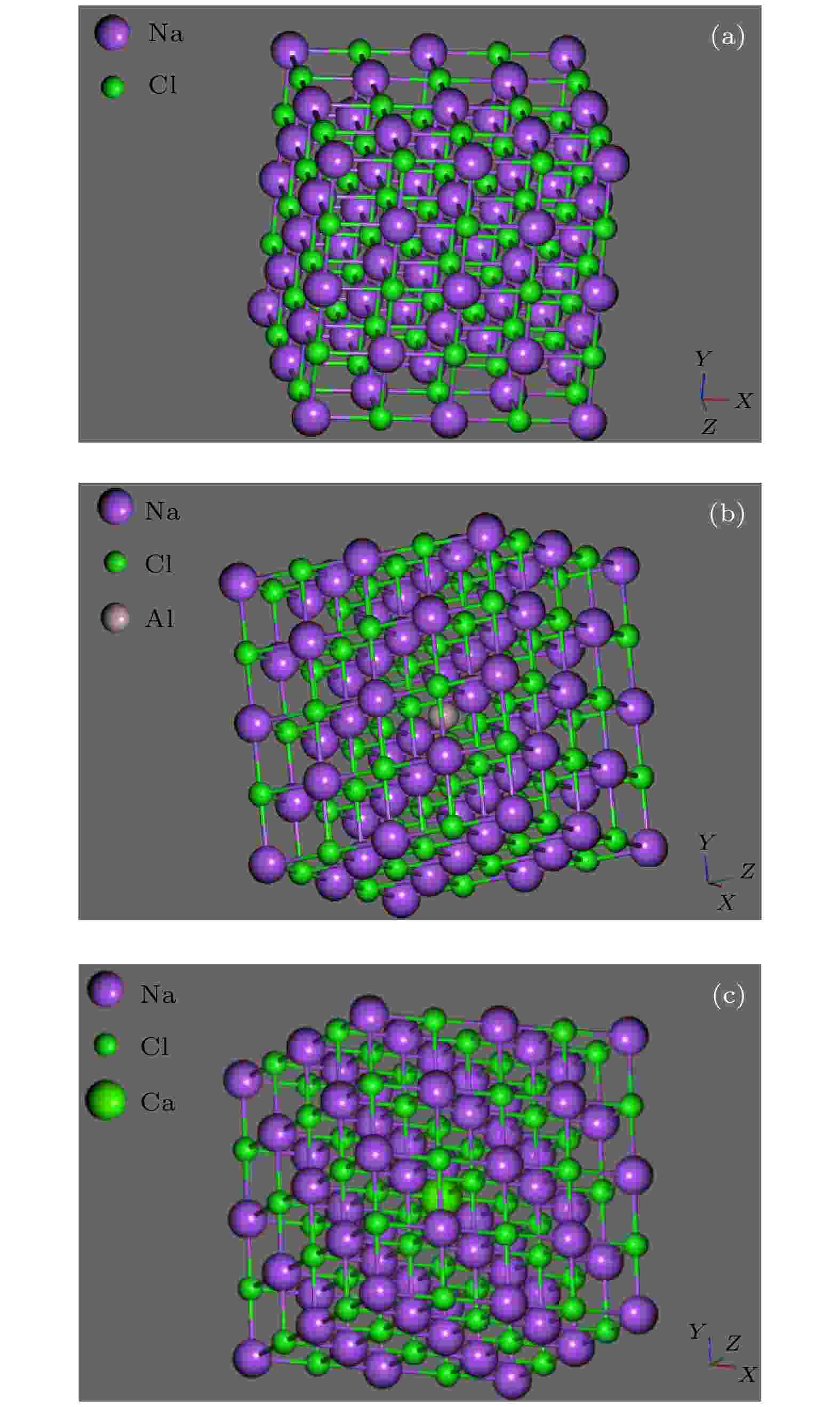
doi:10.7498/aps.73.20240231
Abstract +
To gain a more in-depth understanding of the thermoluminescence peak temperature shift characteristics of pure NaCl itself and its Al and Ca doped variants, a combination of the first-principles calculations and thermoluminescence experiments is used to explore how doping affects the electronic structure of the crystal and further analyze the mechanism of peak temperature shift in thermoluminescence. The calculations indicate that doping NaCl with Al slightly increases its band gap to 5.20 eV, whereas doping with Ca reduces it dramatically to 0 eV. These changes can modify the band gap width but introduce distinct defect formation energy values. Such changes may cause the thermoluminescence peak temperature to occur at lower temperatures and shift with the change of experimental conditions. The theoretical predictions are validated through thermoluminescence experiments, showing that the thermoluminescence peak temperatures of all samples rise with heating rate increasing. Notably, the change is most significant for NaCl:Al, where the peak temperature rises from 276 to 340 K. Meanwhile, as the irradiation dose increases in a range of 1–25 mGy, the growth of the thermoluminescence peak temperature turns relatively small, especially for NaCl:Ca, the peak temperature rises only from 195 to 202 K. This comprehensive analysis of the electronic structures and defect formation energy provides an insight into the thermoluminescence behavior of NaCl crystal. Doping with Al and Ca introduces mid-gap states that act as traps for charge carriers. These traps play a crucial role in the thermoluminescence process, capturing electrons during irradiation and releasing them upon heating, which leads to the observed luminescence. The presence of these traps and their specific energy levels relative to the conduction and valence bands directly influences the temperature at which the peak luminescence occurs. In addition, this study explores how the changes of electronic structure, caused by doping, affects the recombination process of charge carriers, which is very important for the thermoluminescence phenomenon. It also investigates the influence of external factors, such as the rate of heating and the dose of irradiation, on the stability and shift of thermoluminescence peak temperature. These findings emphasize the complex interactions between material composition, structural defects, and experimental conditions in determining the thermoluminescence characteristics of doped NaCl crystals. The results of this research are of great significance for the application of doped materials in various fields, including radiation dosimetry and solid-state lighting. The ability to manipulate the thermoluminescence peak temperatures through doping opens up new ways for designing materials with tailored luminescence properties for specific applications. This study not only deepens our understanding of the fundamental mechanisms of thermoluminescence but also highlights the potential of first-principles calculations combined with experimental analysis in the development of new materials with desired optical and electronic characteristics.

2024, 73 (13): 137803.
doi:10.7498/aps.73.20240445
Abstract +
Black phosphorene (BP) has been widely investigated for its anisotropic and unique photoelectric properties. Strain, voltage and so on are commonly used to modulate the energy band structure and accordingly its photoelectric characteristics. In this study, we consider the energy band structure of BP in the vertical magnetic field, electric field, and in-plane/out-of-plane strains by using the tight-binding approximate Hamiltonian. The anisotropic frequency-dependent interband optical conductivity (IOC) of BP is investigated by using the Kubo formula in these modulation factors. Inherent asymmetry in band dispersion along the armchair (AC) direction and the zigzag (ZZ) direction leads to anisotropic IOC. The introduction of a vertical magnetic field induces band splitting, thereby generating multiple interband transition channels. In this case, the IOC along both the AC direction and the ZZ direction exhibits three peaks around the original peak position, and the magnitudes of the peaks are also modulated. With the increase of in-plane strain (from –20% to 20%), the band gap increases monotonically, and both the position and magnitude of the peaks vary with band gap changing. However, the band gap of BP undergoes a non-monotonic change under out-of-plane strain (from –20% to 20%), which is different from the change under in-plane strain. The band gap reaches a minimum value when a tensile strain of 12% is applied. Along the AC direction, the modulation of the IOC by in-plane strain is opposite to the modulation of out-of-plane strain (εz< 12%), indicating a competitive effect when triaxial strains are applied. Along the ZZ direction, in-plane strain primarily modulates the peak magnitude, while out-of-plane strain effectively modulates not only the peak position but also the peak magnitude obviously. The modulation of the IOC by forward and reverse electric fields are symmetrical. The coefficient for the peak position shift due to the vertical electric field is 1/2 in the AC direction and 1/10 in the ZZ direction. By integrating various modulation factors, we achieve versatile control over the energy band and IOC of BP, providing theoretical support for the application of BP in optoelectronic devices.
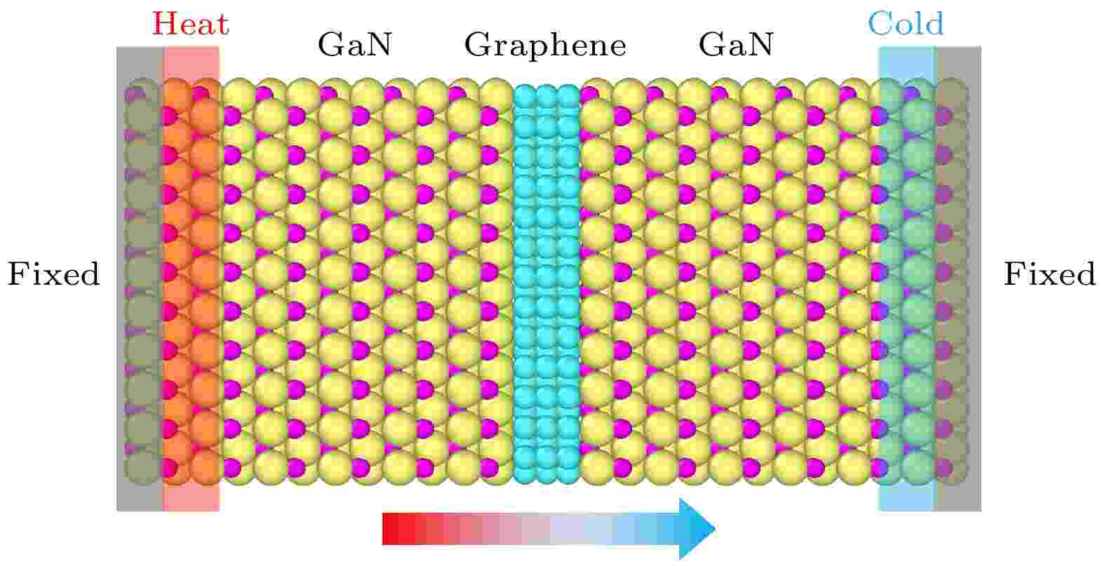
Molecular dynamics study of interfacial thermal transport properties of graphene/GaN heterostructure
2024, 73 (13): 137901.
doi:10.7498/aps.73.20240021
Abstract +
The performance of interfacial thermal transport in heterostructure determines the reliability of micro- and nano-scale device. In this study, a molecular dynamics method is used to investigate the interfacial thermal transport properties of graphene/GaN sandwich heterostructure. The effects of temperature, defect, and size on the interface thermal conductance at the heterostructure are analyzed. It is found that the interface thermal conductance increases with temperature rising; at 1100 K, the interface thermal conductance of the 3-layer graphene heterostructure is increased by 61%. This increase is mainly attributed to the enhanced lattice vibrations at higher temperature, which excites more out-of-plane phonons. The presence of minor vacancy defects in GaN leads interface thermal conductance to increase, reaching a maximum value of 0.0357 GW/(m2·K) at a defect rate of 20%. This enhancement is believed to be due to additional thermal transport pathways created by the defects. However, as the defect rate increases further, the interface thermal conductance begins to decrease, which is thought to be due to interfacial coupling strength decreasing. With the number of GaN layers increasing from 8 to 24, the interface thermal conductance decreases, the change is attributed to the decrease of the number of phonons participating in the thermal transport across the interface. Conversely, with the number of graphene layers increasing from 2 to 6, the interface thermal conductance initially increases and then decreases. This behavior is related to initial improvements of phonon matching and coupling strength, followed by the increase in phonon scattering and localization. The results of this study provide a theoretical basis for regulating the interfacial thermal transport in microelectronic devices.
INTERDISCIPLINARY PHYSICS AND RELATED AREAS OF SCIENCE AND TECHNOLOGY
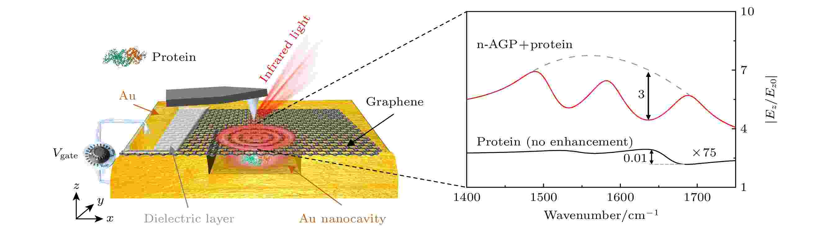
2024, 73 (13): 138101.
doi:10.7498/aps.73.20240489
Abstract +
Nano-infrared spectroscopy (nano-IR) technology can exceed the diffraction limit of light, achieving infrared spectroscopic detection with a spatial resolution of about 10 nm, which is an important technical means for studying the chemical composition and structure of molecules on a nanoscale. However, the weak infrared absorption signals of nanoscale materials pose a significant challenge due to the large mismatch between their dimensions and the wavelength of infrared light. The infrared absorption signals of molecular vibrational modes are proportional to the squares of the electromagnetic field intensities at their positions, implying that higher electromagnetic field intensity can significantly improve the sensitivity of molecular detection. Acoustic graphene plasmons (AGPs), excited by the interaction between free charges in graphene and image charges in metal, exhibit strong optical field localization and electromagnetic field enhancement. These properties make AGPs an effective platform for enhancing nano-IR detection sensitivity. However, the fabrication of graphene nanostructures often introduces numerous edge defects due to the limitations of nanofabrication techniques, significantly reducing the electromagnetic field enhancement observed in experiments. Here, we use finite element simulation to theoretically propose a tunable enhanced nano-IR detection platform based on nanocavity-acoustic graphene plasmons (n-AGPs), which utilizes a graphene/air gap/gold nanocavity structure. This platform avoids needing the nanofabrication of graphene, thereby preventing defects and contamination from being introduced in processes such as electron beam exposure and plasma etching. By plotting the dispersion of n-AGP, it is found that n-AGP has a high wavelength compression capability comparable to AGP (λ0/λAGP= 48). Additionally, due to the introduction of the gold nanocavity structure, n-AGP possess an extremely small mode volume (Vn-AGP≈ 10–7
$ {{ \lambda }}_{0}^{3} $
,λ0= 6.25 μm). By calculating the electric field intensity distribution (|Enorm|) and the normalized electric field intensity spectrum (i.e. the relationship between frequency and |Ez|/|Ez0|) of the n-AGP structure, it is evident that due to the high electron density on the gold surface, electromagnetic waves can be reflected from the boundaries of the gold nanocavity and resonantly enhanced within the nanocavity. At the resonant frequency of n-AGP (1800 cm–1), the electric field inside the cavity is enhanced by about 50 times. In contrast, at similar resonant frequencies, the electric field enhancement factor of Graphene plasmon (resonant frequency 1770 cm–1) and AGP (resonant frequency 1843 cm–1) are approximately 3 and 2 times, respectively, significantly lower than that of n-AGP. Furthermore, by placing a protein film (60 nm wide and 10 nm high) under the graphene, we calculate the spectral dip depths caused by Fano resonance between n-AGP and AGP with the vibrational modes of protein molecules, thereby validating the enhancement factors of different modes for protein vibrational mode infrared absorption. For the amide-I band of proteins, the detection sensitivity of n-AGP is about 60 times higher than that of AGP. Additionally, we find that by adjusting the structural parameters of the gold nanocavity, including cavity depth, width, and surface roughness, the response frequency band of n-AGP can be modulated (from 1290 to 2124 cm–1). Specifically, as the cavity depth increases, the electric field enhancement of n-AGP is improved, and the wavelength compression capability of n-AGP decreases, causing the resonant frequency to be blue-shifted (from 1793 to 2124 cm–1). As the cavity width increases, the resonant frequency of n-AGP is red-shifted (from 1793 to 1290 cm–1), and the effectiveness of the gold nanocavity boundary in reflecting the resonant electric field within the cavity diminishes, resulting in a decrease in the electric field enhancement factor. With the gradual increase in the roughness of the gold nanocavity bottom, the effective depth of the gold nanocavity increases, causing the n-AGP resonant frequency to be blue-shifted (from 1793 to 1861 cm–1) and the electric field enhancement factor to increase. Moreover, by adjusting the Fermi level of graphene (from 0.3 to 0.6 eV), we achieve dynamic tuning of n-AGP (from 1355 to 1973 cm–1). As the Fermi level of graphene increases, the wavelength compression capability of n-AGP decreases, resulting in a blue-shift in the resonant frequency. Finally, by optimizing the structural parameters and Fermi level of n-AGP, and placing protein particles of different sizes (20, 15, and 10 nm high, all 10 nm wide) into the graphene/gold nanocavity structure, we verify the protein detection capability of n-AGP-enhanced nano-IR. We find that n-AGP can detect the vibrational fingerprint features of the amide-I band and amide-II band. For protein films (60 nm wide and 10 nm high), the sensitivity increased by approximately 300 times, and for a single protein particle (10 nm wide and 10 nm high), the sensitivity increased by approximately 9 times. This enhanced structure based on n-AGP holds promise for providing an important detection platform for nanoscale material characterization and single-molecule detection, with broad application potential in biomedicine, materials science, and geology.

2024, 73 (13): 138102.
doi:10.7498/aps.73.20240323
Abstract +
EDITOR'S SUGGESTION
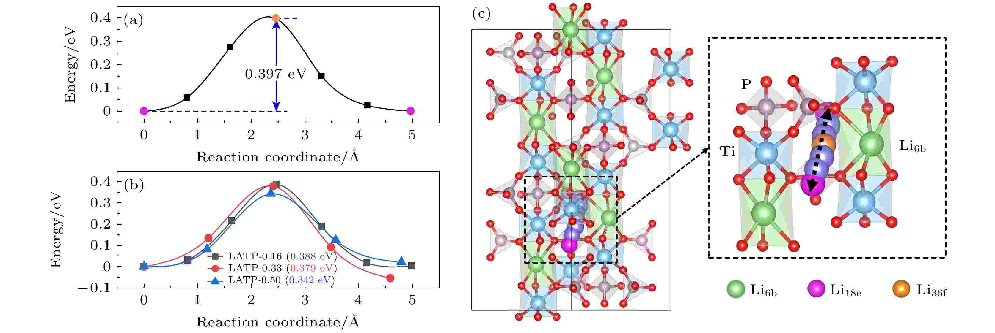
2024, 73 (13): 138201.
doi:10.7498/aps.73.20240044
Abstract +
NASICON-type materials are specific skeleton structures in which ions move in three dimensions. Li1+xAlxTi2–x(PO4)3(LATP) is a promising NASICON-type solid-state electrolyte for Li-ion batteries, due to its relatively high Li+conductivity, chemical stability to air and moisture, and mechanical strength. Motivated by this, we study the doping and electronic properties of Li1+xAlxTi2–x(PO4)3(x= 0.00, 0.16, 0.33, 0.50) and the transport properties of Li+in them by using first-principles calculations based on density functional theory as implemented in Viennaab initioSimulation Package (VASP). The results indicate that Al can substitute Ti to form a stable structure. When the Al doping concentration isx= 0.16, the average bond length of Li—O bond is longest and the bonding strength is weakest, this may lead to the expansion of channels for Li+migration, which facilitates the diffusion of Li+. With the increase of Al doping concentration, the strength of Ti—O bond remains almost unchanged. The electronic structure calculations exhibit that with the increase of Al doping concentration, the bandgap of LATP does not change much, and LATP shows semiconductor characteristic. The differential charge results indicate that more electrons are localized on O-atoms surrounding the Al-dopant, causing the AlO6groups to form polarization centers. The study on the migration properties of Li+indicates that Li+exhibits different migration characteristics in three different migration modes (vacancy migration, interstitial migration, and cooperative migration). With the increase of Al doping concentration, the migration barrier of Li+increases via vacancies involving only lattice site migration, and the migration barrier for LATP-0.16 is lowest (0.369 eV). While in interstitial migration involving only interstitial sites, the migration barrier of Li+decreases accordingly. When the Al doping concentration isx= 0.50, the migration barrier is lowest (0.342 eV). In terms of cooperative migration, this migration mode involves both vacancy and interstitial sites, so the migration barrier first decreases and then increases with the increase of Al doping concentration. Thus, our study suggests that by varying the concentration of Al doping, the interstitial Li+content, migration channel structure, and the migration performance of Li+can be changed favorably. Our results provide a theoretical basis for improving the ion conductivity of Li in LATP by varying the Al doping concentration in experiment.

EDITOR'S SUGGESTION
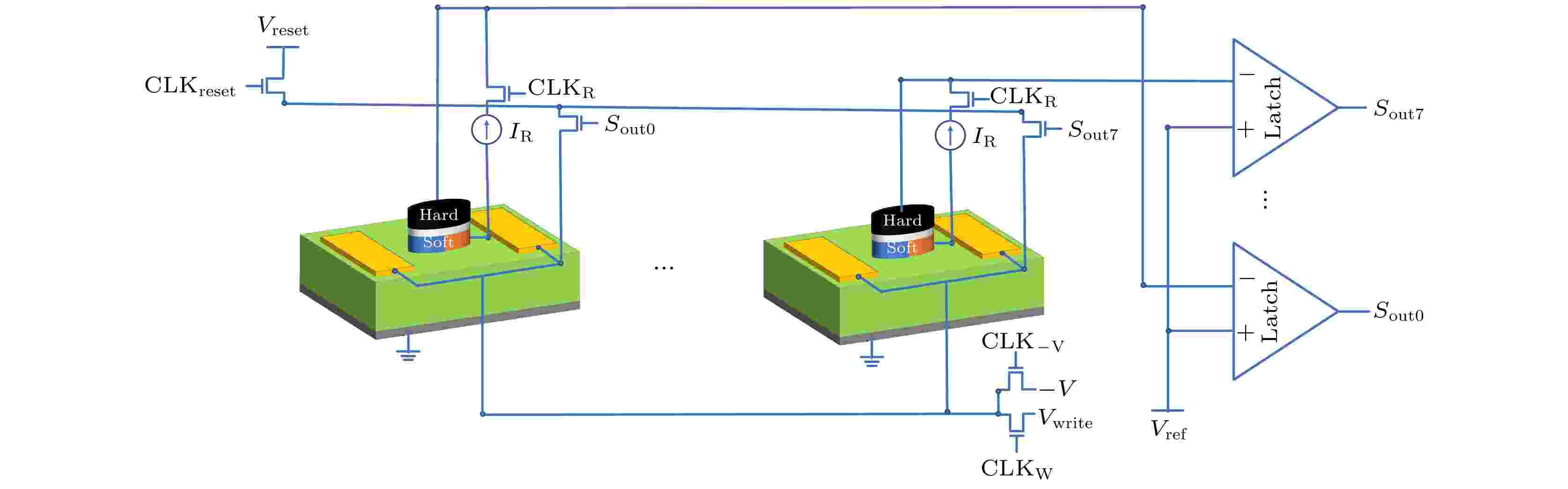
2024, 73 (13): 138501.
doi:10.7498/aps.73.20240398
Abstract +
Superconducting nanowire single-photon detectors (SNSPD) have the advantages of high maximal counting rate (MCR), high detection efficiency, and low dark count rate. They play an important role in the fields of optical quantum communication, optical quantum computing, laser ranging, and imaging. The MCR (i.e. detection speed) of SNSPD can be affected by the front-end readout circuit. To increase MCR, it is usually necessary to use a cryogenic DC-coupled readout circuit with a broad bandwidth. This study reports an SNSPD cryogenic DC-coupled amplification readout circuit based on a commercial high-speed operational amplifier chip OPA855. We systematically characterize its performance parameters in a temperature range from a room temperature of 300 K to a low temperature of 4.2 K. We address the problem of bandwidth loss of the circuit in a low-temperature environment by increasing the operating voltage of the OPA855 chip. For example, at 40 K, the operating voltage increases from ±2.5 V to ±4.9 V, and the quiescent current is about 8 mA, which is equivalent to a power consumption of 78 mW; meanwhile, the gain of this readout circuit is 16.7 dB, and the –3 dB cutoff bandwidth is ~2.7 GHz. We further install a cryogenic DC-coupled readout circuit based on the OPA855 amplifier at 40 K and characterize the performance parameters of the SNSPD at 2.2 K, such as the switching current, system detection efficiency, and MCR. The comparison with the conventional AC-coupled readout circuit at room temperature shows that the MCR increases about 1.3 times after using the DC-coupling circuit. Our study provides the interesting information about the OPA855 amplifier’s performance at low temperatures which facilitates its application in cryogenic environments and related fields.

EDITOR'S SUGGESTION
2024, 73 (13): 138502.
doi:10.7498/aps.73.20240430
Abstract +
For the near-memory computing architecture AI chip manufactured by using 16 nm FinFET technology, atmospheric neutron single event effect irradiation tests are conducted for the first time in China by using the atmospheric neutron irradiation spectrometer (ANIS) at the China Spallation Neutron Source. During the irradiation, the YOLOV5 algorithm neural network running on the AI chip is used for real-time detection of target objects, including mice, keyboard, and luggage. The purpose of the test is to investigate the new single event effect that may occur on near-memory computing architecture AI chip. Finally, at an accumulated neutron fluence of 1.51×10¹⁰n·cm–2(above 1 MeV), a total of 35 soft errors are detected in 5 categories. Particularly noteworthy is the observation of a new finding, where both computing and memory units experience single event effects simultaneously, which is different from the traditional von Neumann architecture chips. Based on the single event effects that occur simultaneously in these two units, combined with Monte Carlo simulation, a preliminary estimation is made of the physical layout distance between the computing unit and the memory unit on the chip. Furthermore, suggestions are proposed to simultaneously reduce the risk of single event effect in multi cells. This study provides valuable reference and insights for further exploring the single event effects in non-traditional von Neumann architecture chips.