Vol. 73, No. 11 (2024)
2024-06-05
The 90th Anniverary ofActa Physica Sinica·COVER ARTICLE
COVER ARTICLE
The 90th Anniverary ofActa Physica Sinica·COVER ARTICLE
COVER ARTICLE
2024, 73 (11): 117802.
doi:10.7498/aps.73.20240512
Abstract +
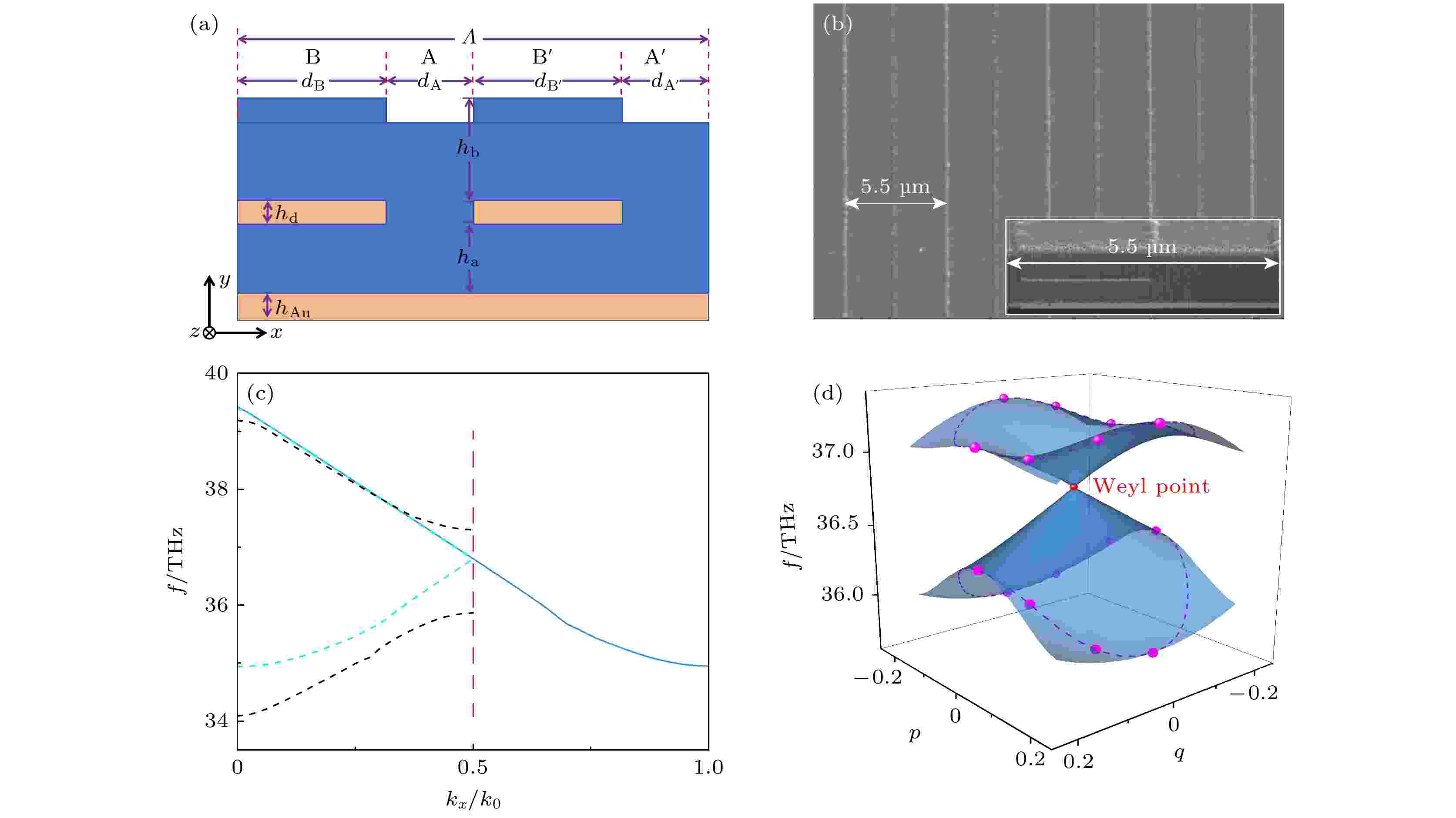
Blackbody emission such as the emission from incandescent sources usually possesses a broadband emission spectrum covering the whole infrared wavelength range. Most of emission energy goes into the unwanted infrared range and consequently causes low emission efficiency. Recently, metasurfaces with two-dimensional subwavelength artificial nanostructures have been widely studied due to their flexibility in modulating optical properties, thus providing an ideal platform for controlling thermal emission. The use of synthetic dimension methods in metasurfaces has opened up new avenues for fine-tuning thermal emission, especially highlighting the physical properties beyond traditional three-dimensional systems and rich topological physics. Although it is theoretically possible to explore physical phenomena through complete three-dimensional structures, such structures are difficult to construct in practice. In contrast, studying one-dimensional system or two-dimensional system is more feasible and efficient. The synthetic dimension approach introduces the possibility of manipulating intrinsic degrees of freedom in photon systems by introducing structural or physical parameters. In this work, we propose utilizing synthetic dimension methods to achieve wavelength-selective thermal emission. Firstly, we construct synthetic Weyl point in a superlattice model and validate it theoretically. Subsequently, experimental characterization of synthetic Weyl cones is conducted by using angle-resolved thermal emission spectroscopy (ARTES). The experimental results demonstrate that we can achieve reasonable wavelength-selective thermal emission while suppressing emission at other wavelengths as much as possible. This is essential for practical infrared applications such as thermalphotovoltaics and thermal management devices.
REVIEW
EDITOR'S SUGGESTION
2024, 73 (11): 110701.
doi:10.7498/aps.73.20240353
Abstract +
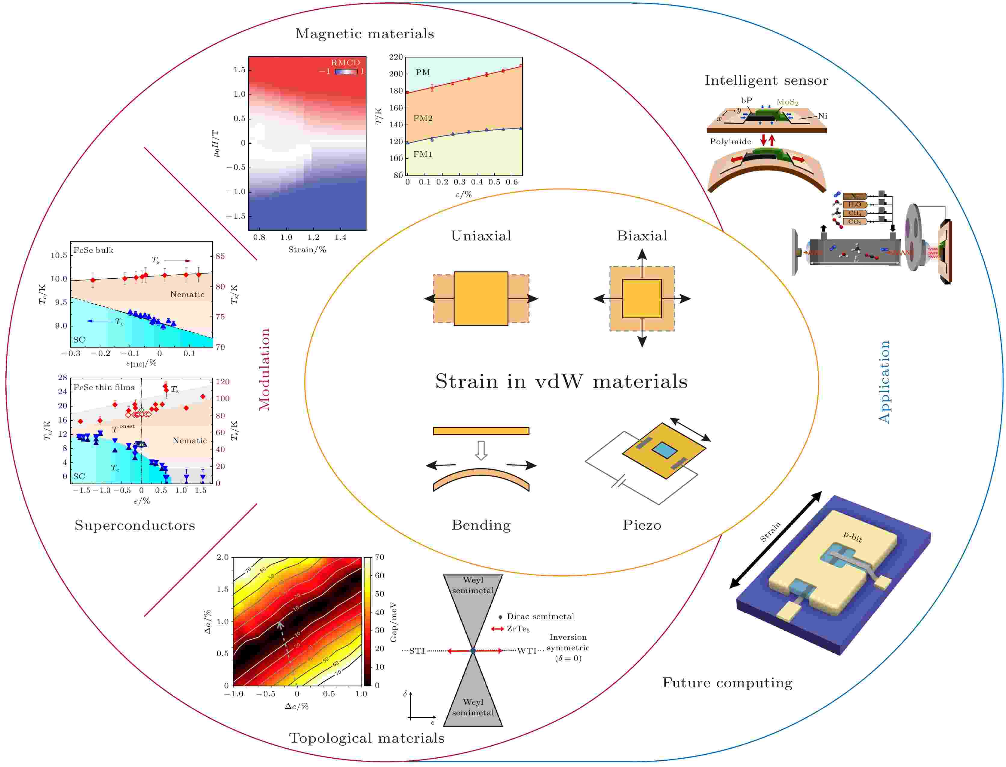
Van der Waals (vdW) materials have attracted extensive research interest in the field of strain engineering due to their unique structure and excellent performance. By changing the atomic lattice and electronic structure, strain can modulate the novel physical properties of vdW materials and generate new quantum states, ultimately realize high-performance electronic devices based on new principles. In this paper, we first comprehensively review various experimental strategies of inducingin-situstrain, which include the bending deformation of flexible substrates, mechanical stretching of microelectromechanical systems and electrodeformation of piezoelectric substrates. Then, we outline the recent research progresses ofin-situstrain-modulated magnetism, superconductivity and topological properties in vdW materials, as well as the development of strain-related device applications, such as intelligent strain sensors and strain-programmable probabilistic computing. Finally, we examine the current challenges and provide insights into potential opportunities in the field of strain engineering.
EDITOR'S SUGGESTION
2024, 73 (11): 117102.
doi:10.7498/aps.73.20240289
Abstract +
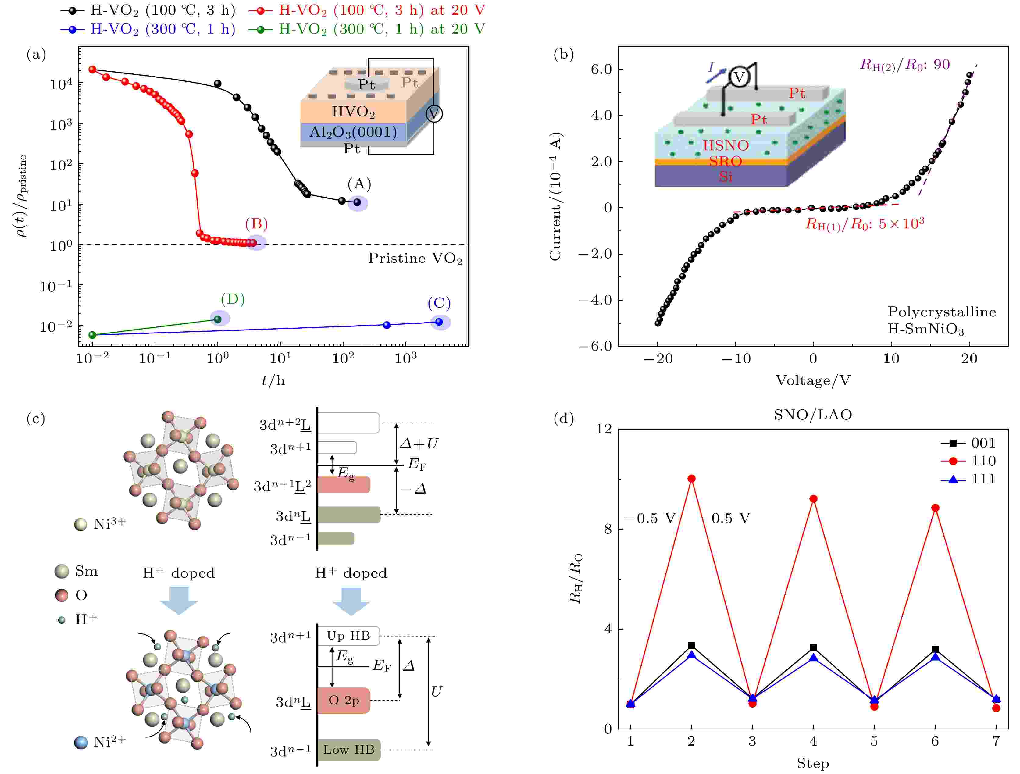
External-field-triggered multiple electronic phase transitions within correlated oxides open up a new paradigm to explore exotic physical functionalities and new quantum transitions via regulating the electron correlations and the interplay in the degrees of freedom, which makes the multidisciplinary fields have the promising application prospects, such as neuromorphic computing, magnetoelectric coupling, smart windows, bio-sensing, and energy conversion. This review presents a comprehensive picture of regulating the electronic phase transitions for correlated oxides via multi-field covering the VO2andReNiO3, thus highlighting the critical role of external field in exploring the exotic physical property and designing new quantum states. Beyond conventional semiconductors, the complex interplay in the charge, lattice, orbital and spin degrees of freedom within correlated oxides triggers abundant correlated physical functionalities that are rather susceptible to the external field. For example, hydrogen-related electron-doping Mottronics makes it possible to discover new electronic phase and magnetic ground states in the hydrogen-related phase diagram of correlated oxides. In addition, filling-controlled Mottronics by using hydrogenation triggers multiple orbital reconfigurations for correlated oxides away from the correlated electronic ground state that results in new quantum transitions via directly manipulating the d-orbital configuration and occupation, such as unconventional Ni-based superconductivity. The transition metals of correlated oxides are generally substituted by dopants to effectively adjust the electronic phase transitions via introducing the carrier doping and/or lattice strain. Imparting an interfacial strain to correlated oxides introduces an additional freedom to manipulate the electronic phase transition via distorting the lattice framework, owing to the interplay between charge and lattice degrees of freedom. In recent years, the polarization field associated with BiFeO3or PMN-PT material triggered by a cross-plane electric field has been used to adjust the electronic phase transition of correlated oxides that enriches the promising correlated electronic devices. The exotic physical phenomenon as discovered in the correlated oxides originates from the non-equilibrium states that are triggered by imparting external fields. Nevertheless, the underneath mechanism as associated with the regulation in the electronic phase transitions of correlated oxides is still in a long-standing puzzle, owing to the strong correlation effect. As a representative case, hydrogen-associated Mottronic transition introduces an additional ion degree of freedom into the correlated oxides that is rather difficult to decouple from the correlated system. In addition, from the perspective of material synthesis, the above-mentioned correlated oxides are expected to be compatible with conventional semiconducting process, by which the prototypical correlated electronic devices can be largely developed. The key point that accurately adjusts and designs the electronic phase transitions for correlated oxides via external fields is presented to clarify the basic relationship between the microscopic degrees of freedom and macroscopic correlated physical properties. On the basis, the multiple electronic phase transitions as triggered by external field within correlated oxides provide new guidance for designing new functionality and interdisciplinary device applications.
GENERAL
2024, 73 (11): 110501.
doi:10.7498/aps.73.20232003
Abstract +
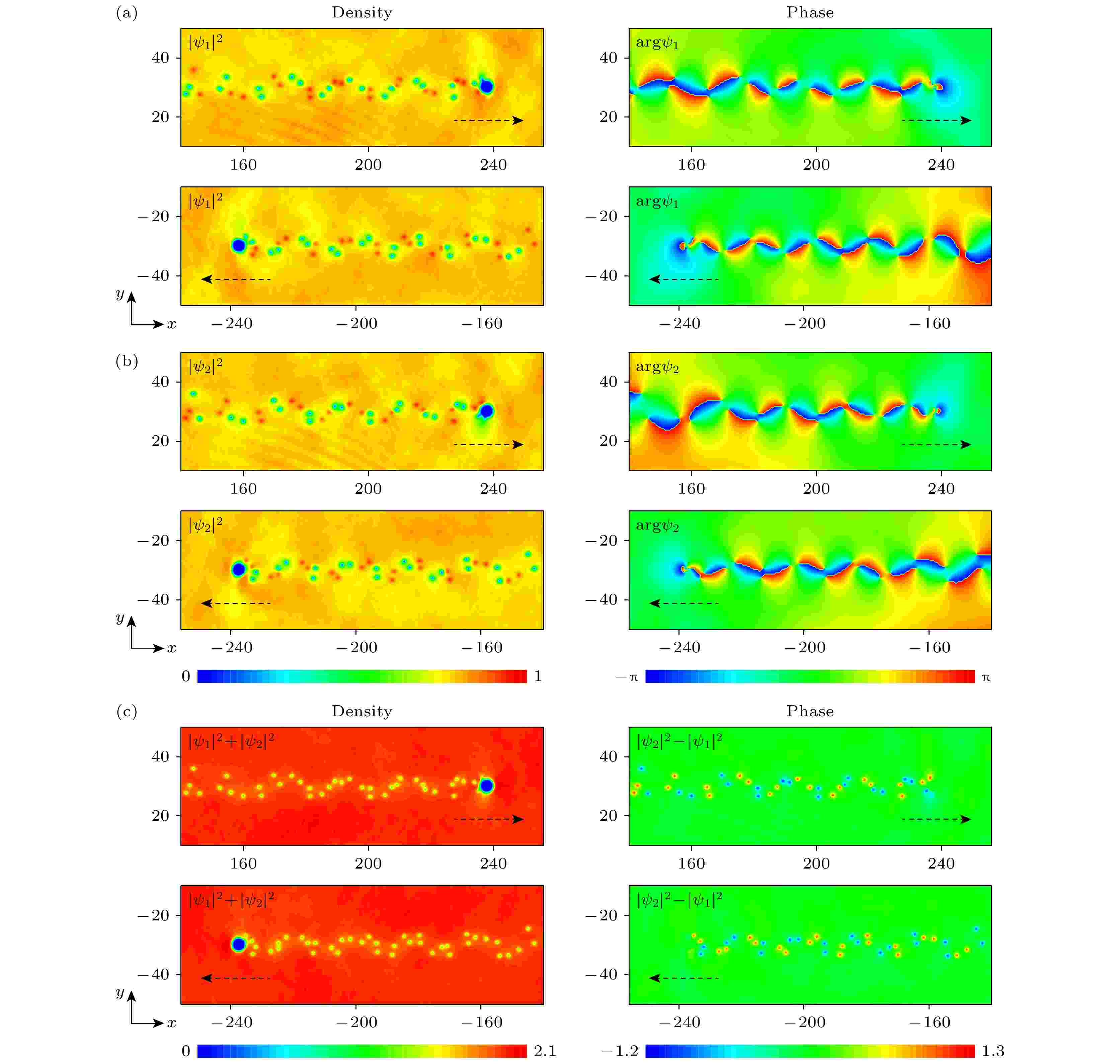
The dynamics of a miscible two-component Bose-Einstein condensate (BEC) with PT (parity-time) symmetric potential are investigated numerically. The dynamical behaviors of the system is described by Gross-Pitaevskii (GP) equations under the mean-field theory. Firstly, the ground state of the system is obtained by the imaginary-time propagation method. Then dynamical behaviors are numerically simulated by the time-splitting Fourier pseudo-spectral approach under periodic boundary conditions. By adjusting the width and velocity of the obstacle potential, various patterns such as no vortex, oblique drifting vortex dipole, V-shaped vortex pairs, irregular quantum turbulence and combined modes are studied. It is noted that the shedding vortex pairs in components 1 and 2 are staggered, which is called “the asynchronous quantum Kármán vortex street”. Here, the ratio of the distance between two vortex pairs in one row to the distance between vortex rows is approximately 0.18, which is less than the stability criterion 0.28 of classical fluid. We calculated the drag force acting on the obstacle potential during generation of the asynchronous quantum Kármán vortex street. It is found that periodical oscillation of the drag force is generated via drifting up or down of the vortex pairs. Meanwhile, we analyzed the influence of the imaginary part of the PT symmetric potential with gain-loss for wake. The trajectory and frequency of the vortex are changed, due to the imaginary part breaks the local symmetry of the system. In addition, the imaginary part affects the stability of the asynchronous quantum Kármán vortex street. Lots of numerical simulations are carried out to determine the parameter regions of various vortex shedding modes. We also proposed an experimental protocol to realize the asynchronous quantum Kármán vortex street in the miscible two-component BEC with PT symmetric potential.
2024, 73 (11): 110502.
doi:10.7498/aps.73.20231133
Abstract +
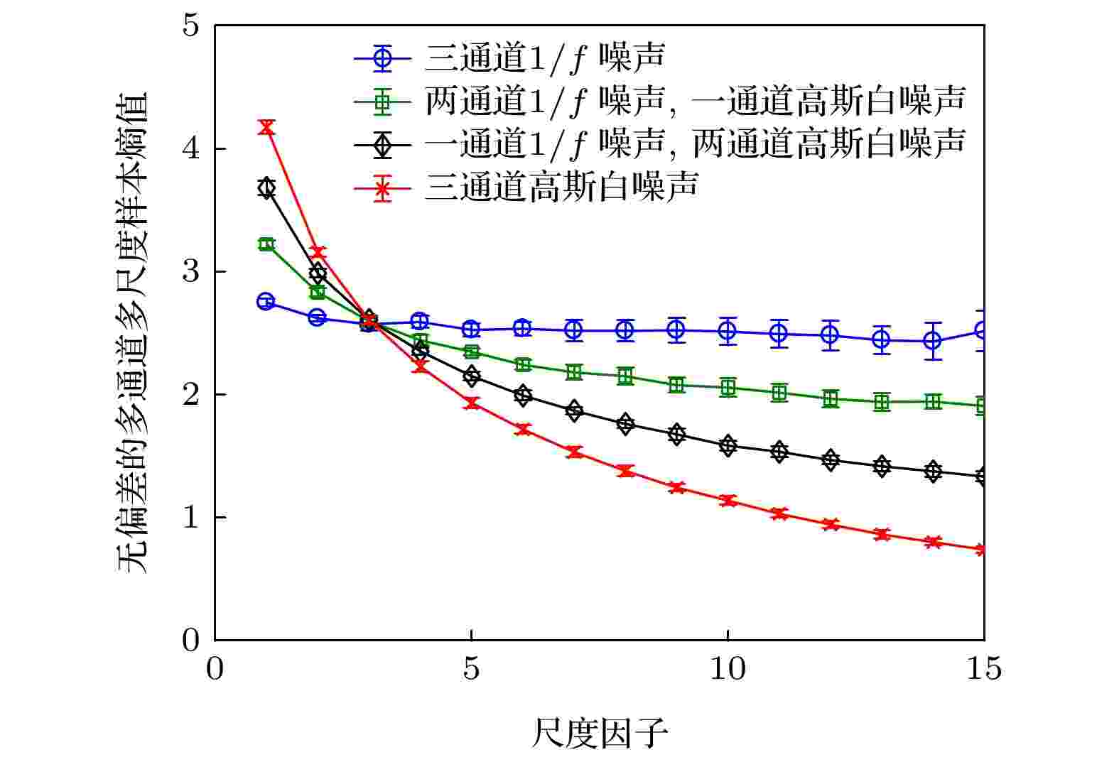
The development of multi-channel data acquisition techniques has provided richer prior information for studying the nonlinear dynamic characteristics of complex systems. However, conventional nonlinear feature extraction algorithms prove unsuitable in the context of multi-channel data. Previously, the multivariate multiscale sample entropy (MMSE) algorithm was introduced for multi-channel data analysis. Although the MMSE algorithm generalized the multiscale sample entropy algorithm, presenting a novel method for multidimensional data analysis, it remains deficient in theoretical underpinning and suffers from shortcomings, such as missing cross-channel correlation information and having biased estimation results. In this paper, unbiased multivariate multiscale sample entropy algorithm (UMMSE) is proposed. UMMSE increases the embedding dimension fromMtoM+p. This increasing strategy facilitates the reconstruction of a deterministic phase space. By virtue of theoretical scrutiny grounded in probability theory and subsequent experimental validation, this paper illustrates the algorithm's effectiveness in extracting inter-channel correlation information through the integration of cross-channel conditional probabilities. The computation of similarities between sample points across different channels is recognized as a potential source of bias and instability in algorithms.Through simulation experiments, this study delineates the parameter selection range for the UMMSE algorithm. Subsequently, diverse simulation signals are employed to showcase the UMMSE algorithm’s efficacy in extracting both within-channel and cross-channel correlation information. Ultimately, this paper demonstrates that the new algorithm has the lowest computational cost compared with traditional MMSE algorithms.
2024, 73 (11): 110503.
doi:10.7498/aps.73.20231972
Abstract +
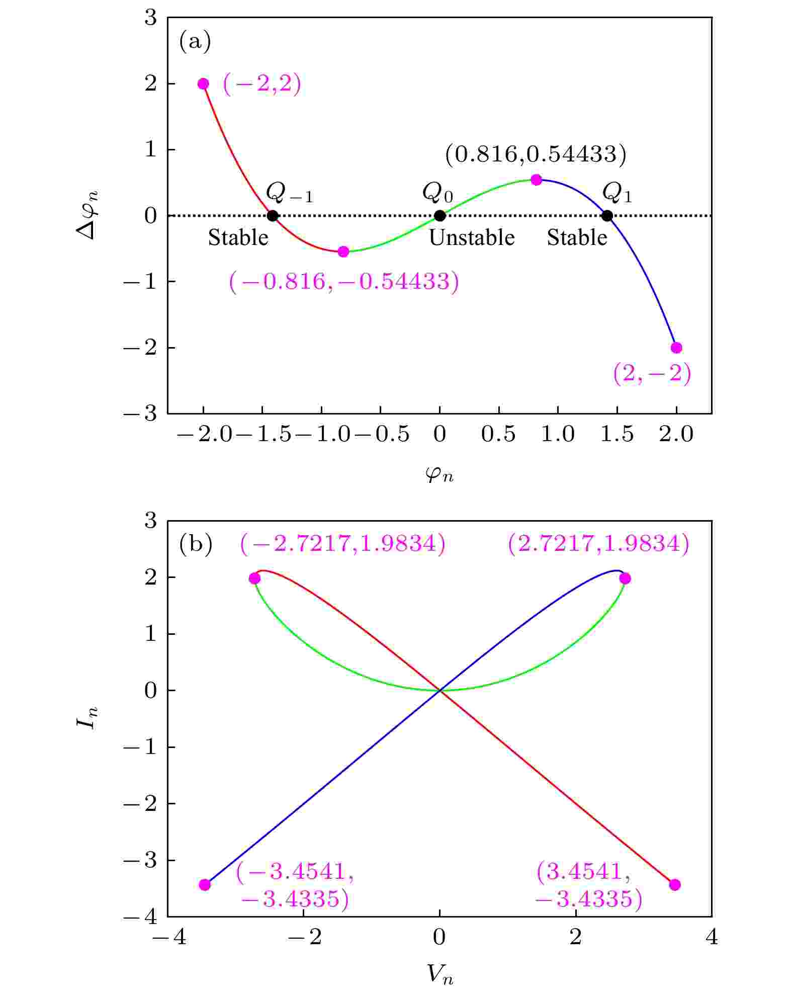
Synaptic crosstalk, which occurs due to the overflow of neurotransmitters between neighboring synapses, holds a crucial position in shaping the discharge characteristics and signal transmission within nervous systems. In this work, two memristors are employed to simulate biological neural synapses and bidirectionally coupled Chialvo discrete neuron and Rulkov discrete neuron. Thus, a heterogeneous discrete neural network with memristor-synapse coupling is constructed, with the crosstalk behavior between memristor synapses in the coupled state taken into account. The analysis demonstrates that the quantity and stability of fixed points within this neural network greatly depend on the strength of synaptic crosstalk. Additionally, through a thorough investigation of bifurcation diagrams, phase diagrams, Lyapunov exponents, and time sequences, we uncover the multi-stable state property exhibited by the neural network. This characteristic manifests as the coexistence of diverse discharge behaviors, which significantly change with the intensity of synaptic crosstalk. Interestingly, the introduction of control parameter into state variables can lead the bias to increase, and also the infinite stable states to occur in the neural network. Furthermore, we comprehensively study the influence of synaptic crosstalk strength on the synchronization behavior of the neural network, with consideration of various coupling strengths, initial conditions, and parameters. Our analysis, which is based on the phase difference and synchronization factor of neuronal discharge sequences, reveales that the neural network maintains phase synchronization despite the variations of the two crosstalk strengths. The insights gained from this work provide important support for elucidating the electrophysiological mechanisms behind the processing and transmission of biological neural information. Especially, the coexisting discharge phenomenon in the neural network provides an electrophysiological theoretical foundation for the clinical symptoms and diagnosis of the same neurological disease among different individuals or at different stages. And the doctors can predict the progression and prognosis of neurological disease based on the patterns and characteristics of coexisting discharge in patients, enabling them to adopt appropriate intervention measures and monitoring plans. Therefore, the research on coexisting discharge in the neural system contributes to the comprehensive treatment of nervous system disease.

EDITOR'S SUGGESTION
2024, 73 (11): 110504.
doi:10.7498/aps.73.20231984
Abstract +
Mesoscopic methods serve as a pivotal link between the macroscopic and microscopic scales, offering a potent solution to the challenge of balancing physical accuracy with computational efficiency. Over the past decade, significant progress has been made in the application of the discrete Boltzmann method (DBM), which is a mesoscopic method based on a fundamental equation of nonequilibrium statistical physics (i.e., the Boltzmann equation), in the field of nonequilibrium fluid systems. The DBM has gradually become an important tool for describing and predicting the behavior of complex fluid systems. The governing equations comprise a set of straightforward and unified discrete Boltzmann equations, and the choice of their discrete format significantly influences the computational accuracy and stability of numerical simulations. In a bid to bolster the reliability of these simulations, this paper utilizes the finite volume method as a solution for handling the discrete Boltzmann equations. The finite volume method stands out as a widely employed numerical computation technique, known for its robust conservation properties and high level of accuracy. It excels notably in tackling numerical computations associated with high-speed compressible fluids. For the finite volume method, the value of each control volume corresponds to a specific physical quantity, which makes the physical connotation clear and the derivation process intuitive. Moreover, through the adoption of suitable numerical formats, the finite volume method can effectively minimize numerical oscillations and exhibit strong numerical stability, thus ensuring the reliability of computational results. Particularly, the MUSCL format where a flux limiter is introduced to improve the numerical robustness is adopted for the reconstruction in this paper. Ultimately, the DBM utilizing the finite volume method is rigorously validated to assess its proficiency in addressing flow issues characterized by pronounced discontinuities. The numerical experiments encompass scenarios involving shock waves, Lax shock tubes, and acoustic waves. The results demonstrate the method's precise depiction of shock wave evolution, rarefaction waves, acoustic phenomena, and material interfaces. Furthermore, it ensures the conservation of mass, momentum, and energy within the system, as well as accurately measures the hydrodynamic and thermodynamic nonequilibrium effects of the fluid system. Compared with the finite difference method, the finite volume method is also more convenient and flexible in dealing with boundary conditions of different geometries, and can be adapted to a variety of systems with complex boundary conditions. Consequently, the finite volume method further broadens the scope of DBM in practical applications.
2024, 73 (11): 110702.
doi:10.7498/aps.73.20232004
Abstract +
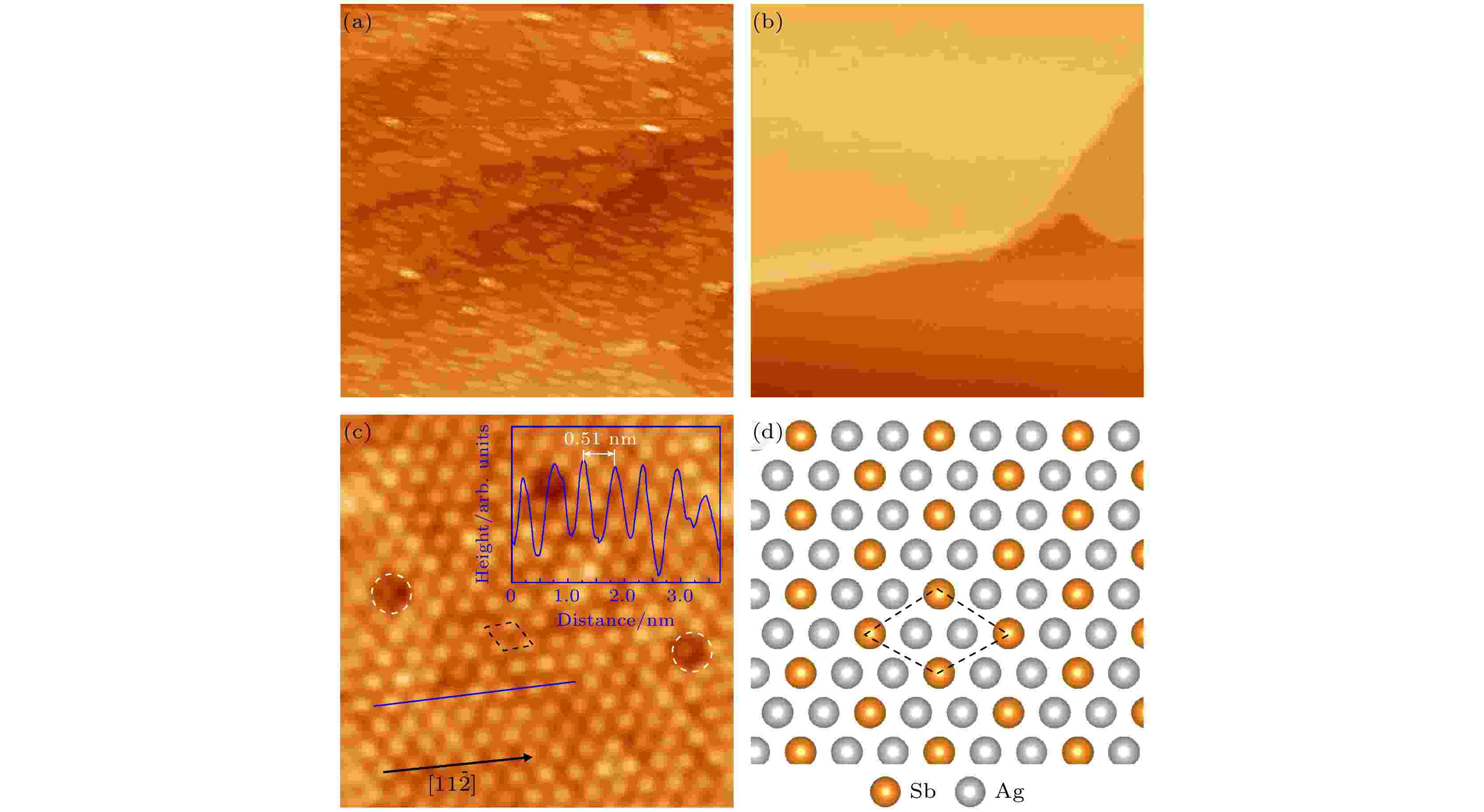
Fabricating ordered molecular films and further tuning their assembly behavior is important for constructing organic devices with diverse performances. By using high-resolution scanning tunneling microscopy, in this work, we demonstrate that well-organized vanadyl phthalocyanine (VOPc) films can be formedvia‘bottom-up’ molecular self-assembly on a binary alloy Ag2Sb/Ag(111). The Ag2Sb monolayer is prepared by evaporating Sb atoms on clean Ag(111) and followed by annealing. The VOPc molecules are deposited on the Ag2Sb layerviathermal evaporation. The molecular configuration, structural and orbital characteristics of VOPc are clearly clarified at a submolecular level. It is found that initially the ordered VOPc membrane only exhibits the O-up adsorption configuration. Its square-shaped unit cell consists of five VOPc molecules where two adsorption orientations coexist with the horizontal axis of VOPc which is rotated by about 11° or 21° relative to the side of the unit cell. Due to the molecular dipole-dipole interaction, further-deposited molecules result in the assembly of the second-layer VOPc films with the O-down configuration and the square-shaped unit cell that contains only one VOPc molecule. Subsequently, due to the dipole-dipole interaction between layered molecules, following VOPc molecular layers adopt alternating O-up and O-down configurations as well as the square-shaped unit cell, similar to the case of the second layer. In addition, we find that the molecular orbitals overlap in each assembled molecular layer due to the π-π interaction which could facilitate the charge transport along the π stacking direction of VOPc. This research provides possibility to regulate the adsorption configuration and assembly behavior of functional organic molecules on metal surfaces by forming surface alloys.
NUCLEAR PHYSICS
2024, 73 (11): 112301.
doi:10.7498/aps.73.20240212
Abstract +
2024, 73 (11): 112801.
doi:10.7498/aps.73.20240007
Abstract +
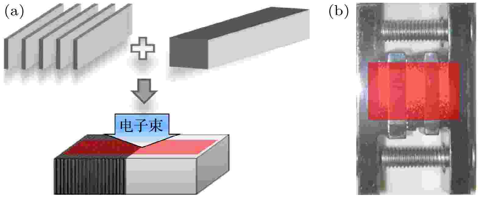
The response of tungsten (W) to thermal shock loading, as the best candidate for plasma-facing material (PFM), is an important issue in the research of future fusion devices. Under thermal loading, thermal irradiation damage, including brittle cracking and fatigue cracking, occurs on the surface of tungsten based plasma-facing material (W-PFM). In this work, a new scheme to suppress the thermal irradiation damage to W-PFM, i.e. the laminated structure W-PFM scheme, is proposed. Thermal fatigue experiments of laminated structure W composed of W foils with different thickness and heat treatment processes are carried out by using an electron beam device. The samples are subjected to thermal pulses with a power density of 48 MW/m2for 5000 cycles. The results indicate that the crack damage to the surface of the laminated structure W decreases with the decrease of the thickness of W foils under the same heat treatment conditions. The main cracks are produced on the surface of laminated structure W after cyclic thermal loads have been all approximately parallel to the foil thickness direction. Only the main cracks appear on the surfaces of W foils with a smaller thickness, while crack networks develop on the surfaces of W foils with a larger thickness , in addition to the main cracks with a larger width. In the rolled state, the laminated structure W has the lowest degree of surface plastic deformation for the same thickness. The thermal fatigue crack damage to the surface is quantitatively analyzed by using computer image processing software and analysis software, and scanning electron microscope images of the thermal damage area are finally selected. It is found that the de-stressed state W has the smallest crack area and the smallest number of cracks for the same thickness, indicating that the de-stressed state W has the strongest resistance to irradiation damage. The experimental results also show that in addition to the effect of microstructure, both the uniaxial stress state and the crack-blocking mechanism of the laminated structured W-PFM contribute to the improvement of its thermal fatigue performance.
ATOMIC AND MOLECULAR PHYSICS
2024, 73 (11): 113101.
doi:10.7498/aps.73.20231681
Abstract +
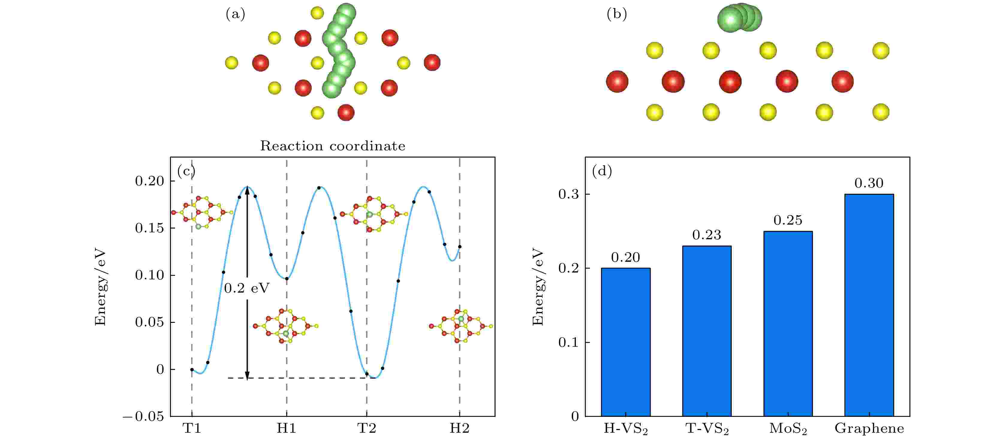
With the increase of performance requirements for lithium-ion batteries (LIBs), it is particularly important to study and develop new electrodes for lithium-ion batteries. In this work, a 3×3×1 supercell of VS2is constructed, and the possibility of using it as an anode material for lithium-ion batteries is study by the first-principles method based on density functional theory. Through the analysis of the energy band diagram, it is found that VS2has metallic properties. Combining the density of states diagram, the analysis shows that the energy band near the Fermi level of VS2is contributed by the 3d state of V and the 3p state electrons of S, which means that the conductive properties of VS2are largely affected by the 3d state of V and the 3p state electrons of S. Of the vacancies, bridge sites, and top sites of lithium adsorbing vanadium (V), the top site has the lowest adsorption energy, indicating that lithium will preferentially adsorb the top site of vanadium (V). Through first-principles molecular dynamics simulations of the top position of adsorbed vanadium (V), it is found that at a temperature of 300 K, the total energy of the system and the magnitude of the total temperature fluctuation can reach a steady state, indicating that lithium can exist at the top position of stably adsorbed vanadium (V). Moreover, the interlayer spacing of the double-layer VS2reaches 3.67 Å, which is larger than the interlayer spacing of graphene. From the top position to the vacancy, its diffusion barrier is only 0.20 eV. Its interlayer spacing is larger than the double-layer graphene’s, and its diffusion barrier is lower than graphene’s, indicating that lithium has very good diffusivity on the VS2surface, and lithium can migrate quickly on the VS2surface, which is conducive to the rapid charge-discharge process of LIB. In addition to excellent electrical conductivity, VS2has good mechanical properties. The calculated Young's modulus is 96.82 N/m, and the Young's modulus and Poisson’s ratio do not decrease after adsorbing lithium, indicating that the rigidity of VS2will not be reduced in the diffusion and migration process of lithium. On the other hand, it has excellent deformation resistance. In order to be more accurate and closer to the actual situation, a double-layer VS2model is constructed, with a maximum number of lithium atoms adsorbed between layers being 18. The calculated theoretical capacity of VS2(466 mAh/g) is higher than the theoretical capacity of graphene (372 mAh/g). Our results indicate that VS2has excellent electrical conductivity and mechanical stiffness, making it a promising cathode material for lithium-ion batteries.
2024, 73 (11): 113201.
doi:10.7498/aps.73.20240355
Abstract +
EDITOR'S SUGGESTION
Atoms loading and cooling for an optical cavity assisted by Λ-enhanced gray-molasses cooling process
2024, 73 (11): 113701.
doi:10.7498/aps.73.20240182
Abstract +
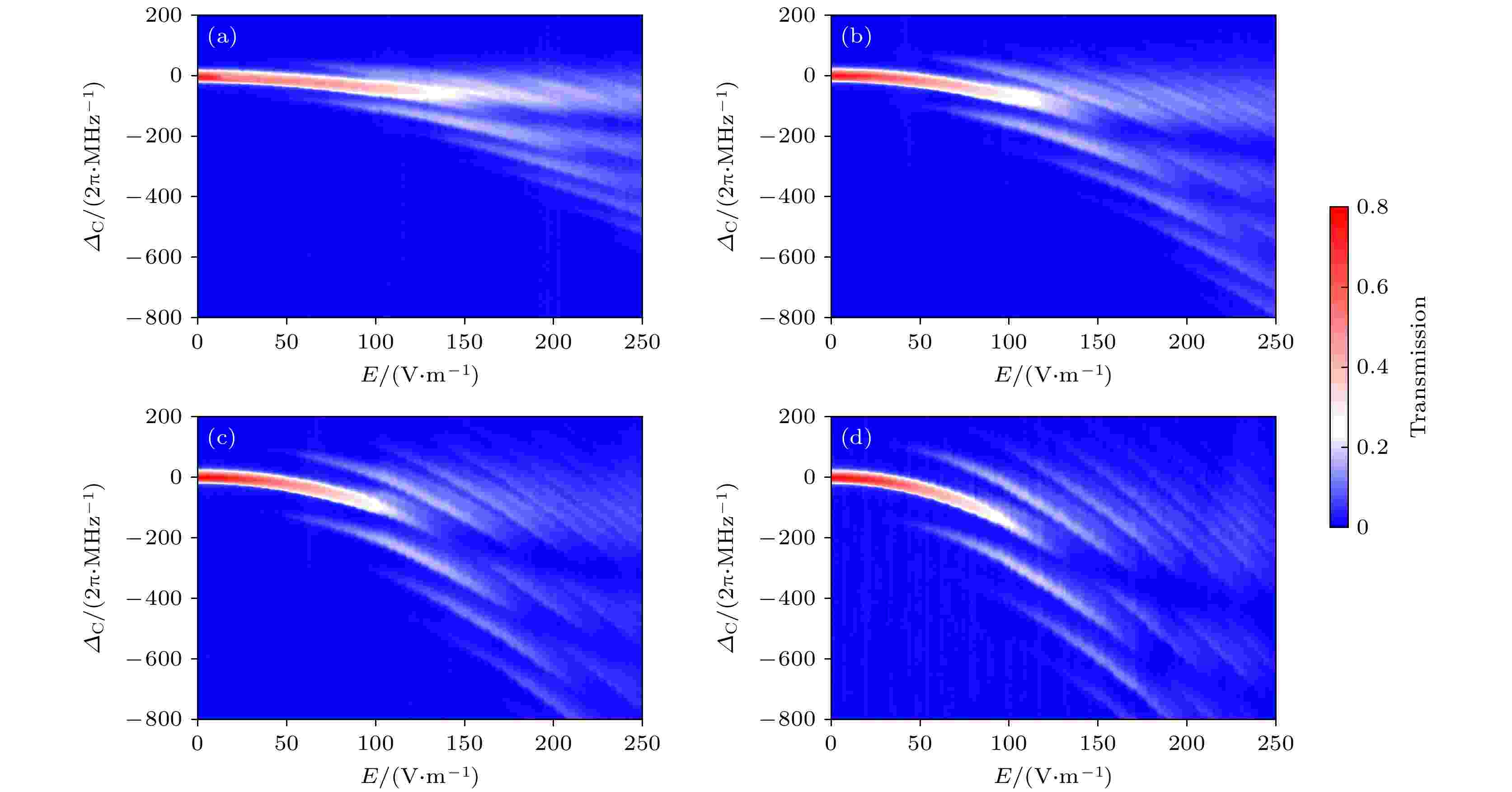
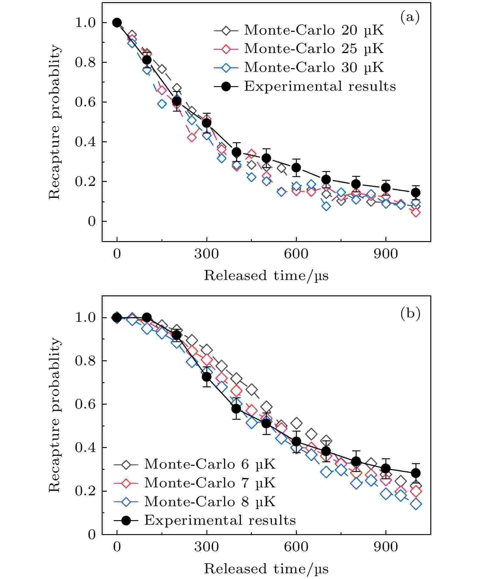
Λ-enhanced gray molasses cooling (Λ-GMC) technique has been widely used in experiments to prepare cold atomic samples below the sub-Doppler temperature limit. To meet the experimental requirements of cavity quantum electrodynamics systems, we design and construct a wide-range, fast-tuning laser system by integrating tapered amplifiers, fiber phase modulators, etalon, injection locking amplification techniques etc. This laser system achieves a maximum tuning range of 600 MHz and a frequency tuning speed of 5 ns. Based on this laser system, loading atom in a crossed dipole trap assisted by cesium D2 line Λ-GMC cooling in the center of the optical microcavity is studied, and various factors affecting the atom loading are mainly as follows: laser duration
$\tau $
, three-dimensional magnetic field
$ \left( {{B_x}, {B_y}, {B_z}} \right) $
, single-photon detuning
$\varDelta $
, two-photon detuning
$\delta $
, ratio of cooling beam power to repumping beam power
${I_{{\text{cool}}}}/{I_{{\text{rep}}}}$
, and cooling beam power
${I_{{\text{cooling}}}}$
. The optimal parameters in this system are follows:
$ \tau = 7{\text{ ms}},\; \delta = 0.2{\text{ MHz}},\; \varDelta = 5\varGamma, \;{I_{{\text{cool}}}}/{I_{{\text{rep}}}} = 3, {\text{ and }} {I_{{\text{cool}}}} = 1.2{I_{{\text{sat}}}}. $
Comparing with traditional PGC-assisted loading, the number of atoms is increased about 4 times, and the atomic temperature decreases from
$ 25{\text{ μK}} $
to
$ 8{\text{ μK}} $
. This experiment provides important insights for preparing ultracold atomic samples and capturing single atom arrays.
ELECTROMAGNETISM, OPTICS, ACOUSTICS, HEAT TRANSFER, CLASSICAL MECHANICS, AND FLUID DYNAMICS

2024, 73 (11): 114201.
doi:10.7498/aps.73.20240335
Abstract +
2024, 73 (11): 114202.
doi:10.7498/aps.73.20231906
Abstract +
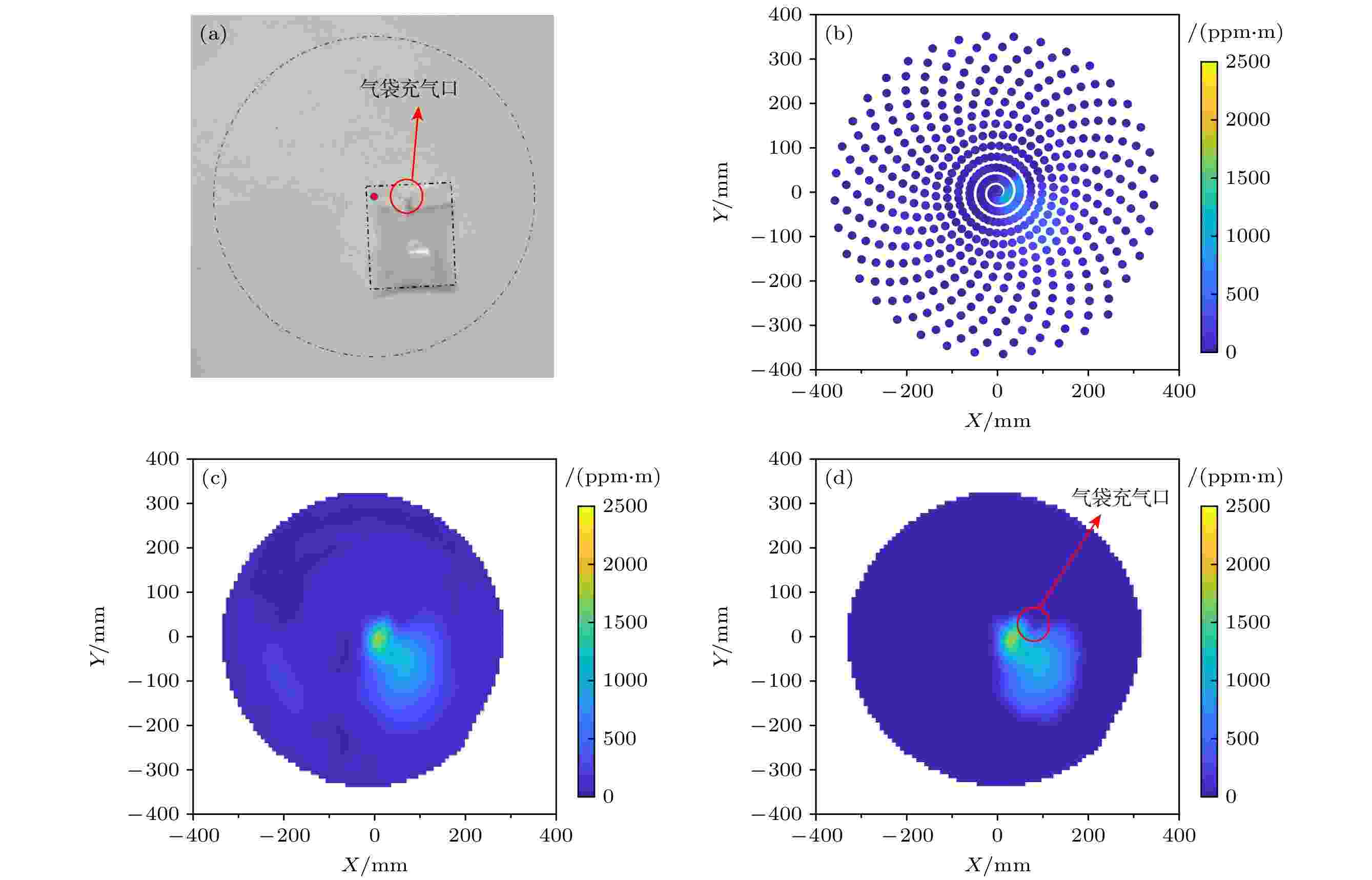
With the increase in the number of oil and gas pipelines laid in China, more attention needs to be paid to pipeline maintenance work. At present, the main methods of detecting natural gas leaks in oil and gas transmission stations include manual inspections, opposing natural gas detection equipment, and cloud desktop natural gas detection equipment. Hand held natural gas detection equipment is used for manual inspection, which requires regular manual inspection. However, the response speed is poor and gas leaks cannot be detected in a timely manner. The opposed laser gas detection method can only detect the presence of gas on the beam path. If a larger area of leakage detection is desired, more equipment needs to be installed, resulting in a greatly increase in hardware costs. The existing cloud desktop laser gas detection method controls the deflection of the laser beam through the cloud platform to achieve leak detection at various points in the area to be tested. However, the rotation speed of the cloud platform is slow, and a complete detection cycle takes dozens of minutes, and only the presence of gas can be detected. For accurate leak location, manual on-site survey is also required to further determine the leak location. In order to meet the needs of the real-time monitoring and rapid positioning of oil and gas pipeline leaks, in this work, a fast and accurately controlled dual wedge scanning mirror system is designed, which combines tunable semiconductor laser absorption spectroscopy technology to convert the gas measurement laser beam from point measurement to surface measurement, thereby obtaining the two-dimensional distribution of gas, which is conducive to subsequent analysis and positioning of gas leakage sources. By using the inverse solution iterative optimization algorithm, the angle of the wedge mirror is controlled to obtain an efficient and uniform beam scanning trajectory. The deflection direction and detection position of the laser beam are fused with the corresponding methane concentration information, and a methane concentration data containing position information is constructed. In order to quantitatively verify the measurement accuracy and spatial resolution in the experiment, a standard air bag is used to simulate the methane leakage distribution. The results show that the minimum detection limit of the system can be lower than 5×10⁻⁴m, and the spatial resolution can be less than 6 cm. At the same time, this method can adjust the scanning step node based on the measurement distance of the oil from gas station, thereby achieving adjustable imaging resolution. This imaging method provides a new idea for accurately positioning and detecting the methane leakage location and amount.
2024, 73 (11): 114203.
doi:10.7498/aps.73.20240279
Abstract +
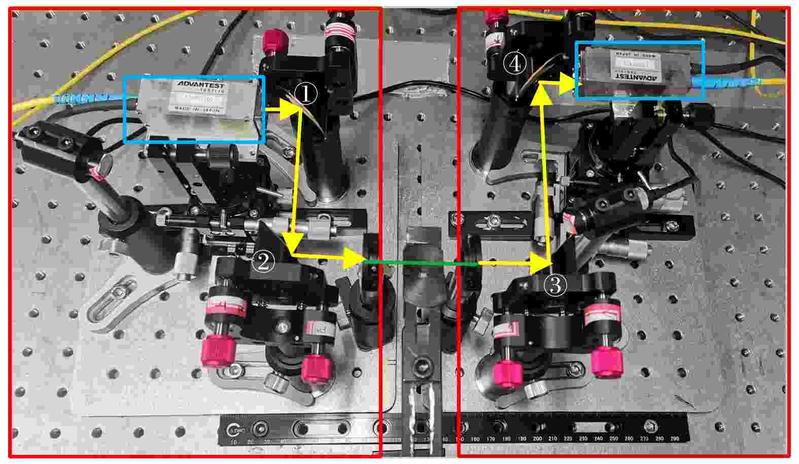
Terahertz waves are between microwave and infrared, and currently, terahertz waves are mainly transmitted in free space. Metal wire waveguides have been widely studied due to their outstanding transmission characteristics such as low loss and low dispersion. In this study, copper wires are selected as the research samples based on the skin depth of terahertz waves on different metal wire surfaces. An adjustable metal wire waveguide transmission characteristic testing optical path is studied based on the terahertz time-domain spectroscopy system. The time-domain signals transmitted through single/double copper wires with different radii, lengths, and port states are collected. Then, the finite element method is used to analyze the transmission characteristics of single/double copper wires with different radii, lengths, and port states, and the transmission characteristics of single/double copper wires with different degrees of deformation in the air domain are simulated. The experimental results indicate that the transmission loss increases with copper wire length increasing, and the thinner the metal wire, the slower the transmission speed is. The influence of port shape on transmission characteristics is not so significant as that of length variation. The thicker the bimetallic wire, the faster the transmission speed is. The simulation results show that when terahertz waves are transmitted on a single metal wire, the electric field is mainly distributed on the surface of the metal wire, and the finer the metal wire, the smaller the mode field area of the surface plasmon is. When the metal line becomes elliptical, the mode field is mainly distributed on both ends of the major axis; When terahertz waves are transmitted in bimetallic wires, the mode field is mainly distributed between the two wires, and the farther the distance, the smaller the mode field area is. In this work, the terahertz transmission characteristics of single wires and bimetallic wires are studied by combining experimental method and simulation analysis, providing a reference for the subsequent development of efficient terahertz metal waveguides.
2024, 73 (11): 114301.
doi:10.7498/aps.73.20240250
Abstract +
2024, 73 (11): 114401.
doi:10.7498/aps.73.20240089
Abstract +
2024, 73 (11): 114601.
doi:10.7498/aps.73.20240333
Abstract +
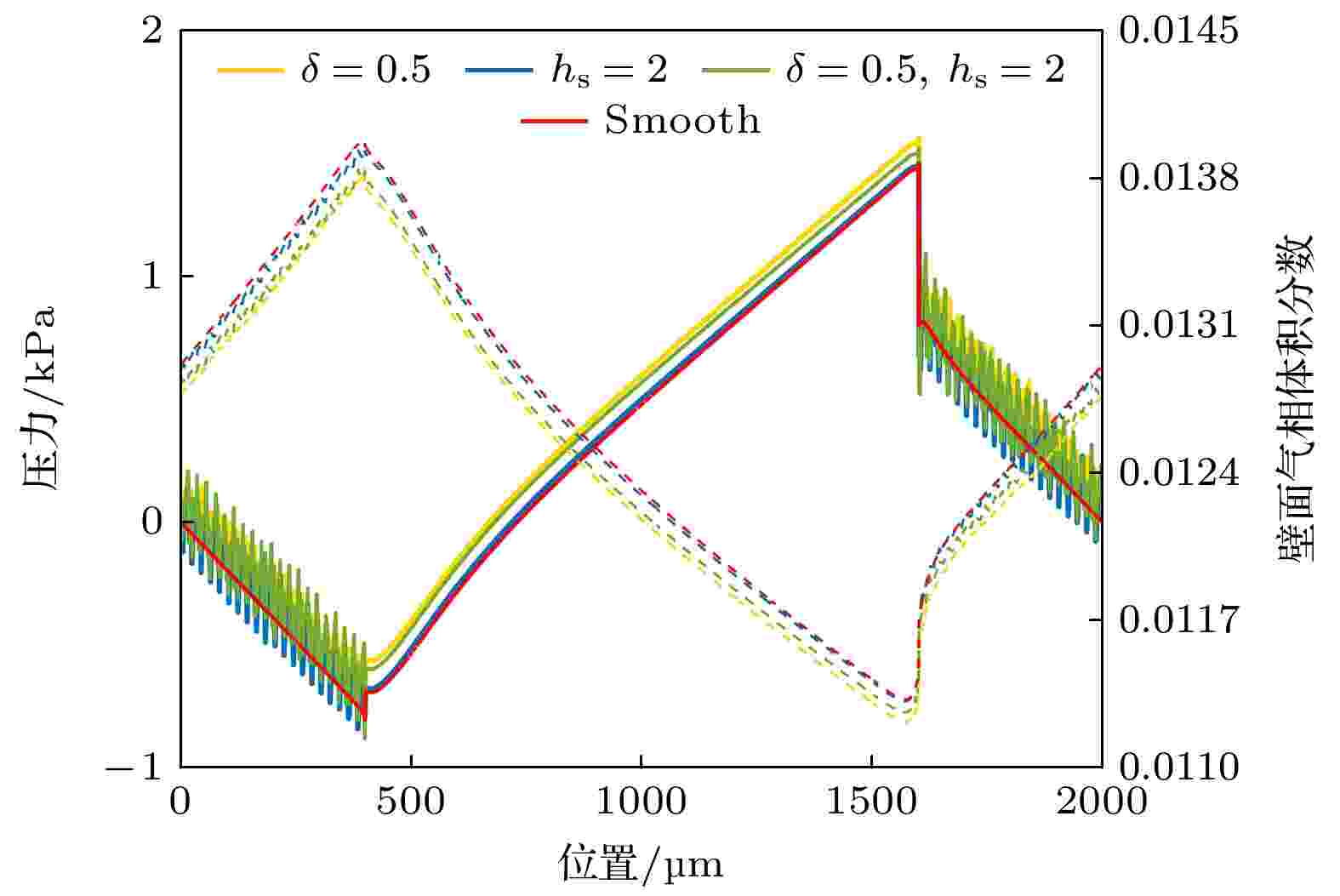
With the development of surface precision machining technology and extensive studies on lubrication and friction reduction, the use of surface texture to reduce friction has attracted widespread attention, but few studies have considered the influence of surface roughness on lubrication characteristics. By employing the computational fluid dynamics (CFD) simulation method, the lubrication models with rectangular textures and the introduction of rough asperity structures at the same time are established. The effects of the corresponding structure parameters on the lubrication performance of textured and roughed surfaces are studied under water lubrication conditions. Our results suggest that the adjustment of geometric parameters on the micro-/nano-structured surfaces can influence the load-bearing capacity of the water lubrication film, thus affecting the hydrodynamic lubrication performance on the surface. In addition, the generation of vortex in the micro-textures can bring changes in vorticity, which causes energy dissipation and affects frictional forces. In the lubrication model with rectangular textures, optimal hydrodynamic lubrication performance is obtained under the appropriate depth ratioH= 0.6. Meanwhile, the corresponding lubrication performance can be enhanced by increasing the width ratio (W) of surface texture. After introducing random asperity structures on the micro-textured surface with a standard deviationδ= 0.5, the bearing capacity is increased by 44%, and the friction coefficient is reduced by 30.9%. Moreover, the introduction of half-sine rough asperity structures can only result in relatively minor differences in the lubrication performance, i.e. the changes of bearing capacity and friction coefficient are less than 10%. However, the introduction of compound hierarchical structure consisting of random asperity structures and half-sine rough asperity structures can result in an increase in the corresponding bearing capacity by 42% and a reduction in the friction coefficient by 31.1%, which implies a significant enhancement in the hydrodynamic lubrication performance.
2024, 73 (11): 114701.
doi:10.7498/aps.73.20231893
Abstract +
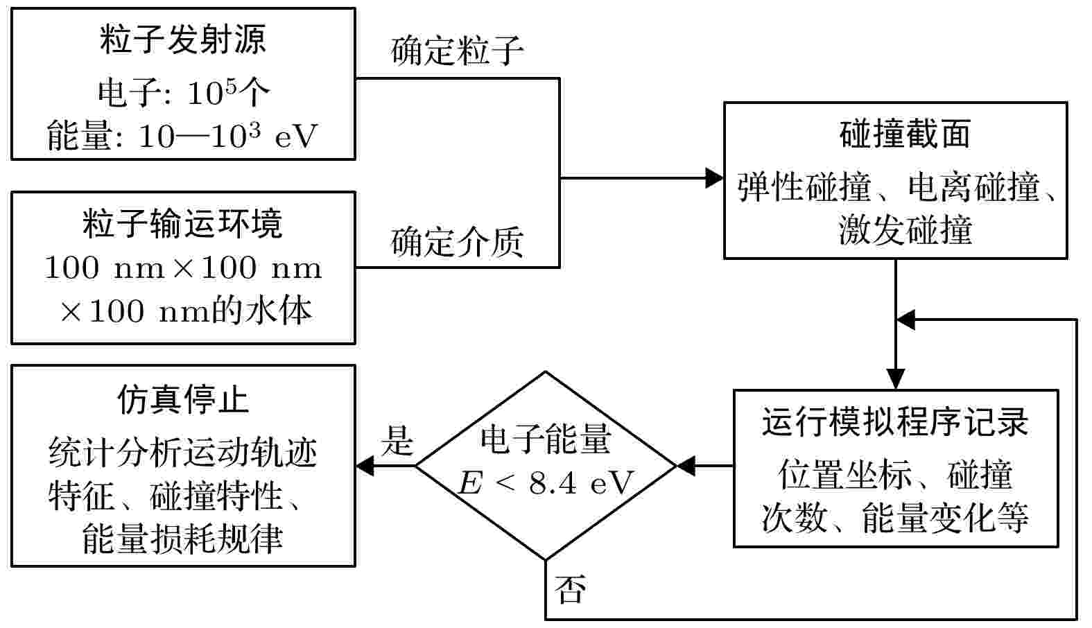
The transport characteristics of electrons are crucial for the initiation and development of pulse discharge in water. In this work, we develop a physical model of electron transport that consides elastic and inelastic collision cross sections. The purpose of this study is to investigate frequency variations of elastic collisions, ionization and excitation collisions with different initial electron energy values, and to explore the characteristic of electron energy loss in water. The Monte Carlo method is employed to track structure characteristics of electron transmission and scattering under varying energy values. The results show that the electrons of lower energy (~20 eV) are significantly impacted by the water molecule scattering, hence their transmission capacities are weakened. When the incident energy of electron reaches 100 eV, the scattering deviation distance is roughly equivalent to the transmission depth, about 6–8 nm, and the maximum deviation angleθshift~ 60°. When the electron incident energy is in a range of 10–1000 eV, the number of elastic collisions is much greater than the number of excitation and ionization collisions, and the number of ionization collisions and excitation collisions increases significantly with the increase of electron energy. The higher the electron incident energy, the greater the energy loss is. However, the energy loss decreases sharply with the extension of penetration distance. For the ionization collision, the average ionization energy loss,W, decreases rapidly with the increase of electron energy, and ultimately maintains at a level of 20–30 eV, which is consistent with the experimental results reported.
PHYSICS OF GASES, PLASMAS, AND ELECTRIC DISCHARGES
2024, 73 (11): 115201.
doi:10.7498/aps.73.20240319
Abstract +
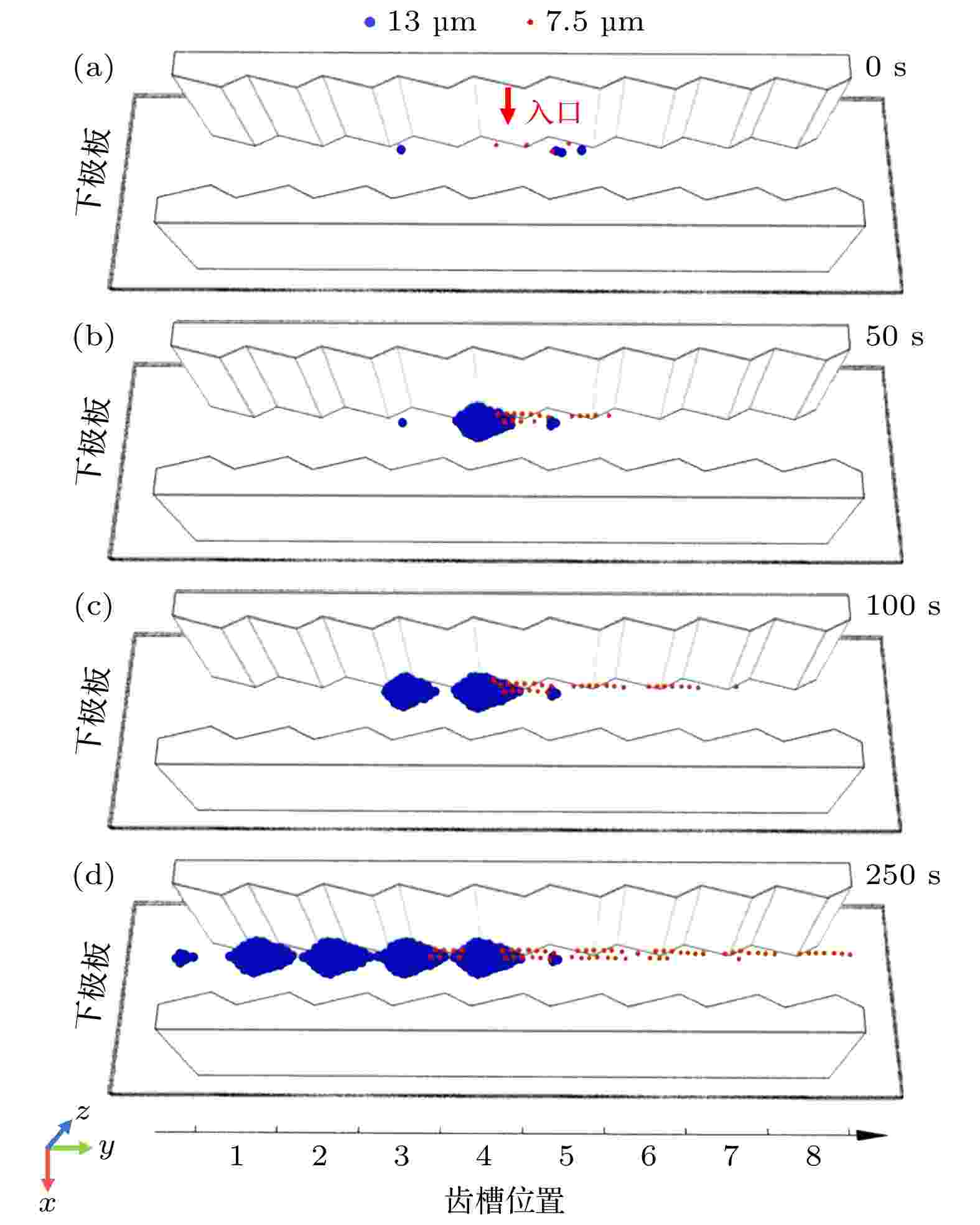
A ratchet can be employed to rectify randomly moving particles, generating directional transport. Taking advantage of the distinct responses of particles with different sizes to the system, bi-dispersed particles can be effectively separated. Based on previous experiments demonstrating the rectification and separation of dust particles in gas-phase plasma, a three-dimensional model is constructed to reveal the physical mechanism behind the separation of bi-dispersed dust particles here. Utilizing plasma fluid simulation and double sine function interpolation, the distribution of plasma parameters in the asymmetric ratchet channel is obtained, which is challenging to measure experimentally. Subsequently, a numerical simulation of the directional transport process of bi-dispersed dust particles in a dusty plasma ratchet is conducted by solving the Langevin equation. The results analyze the forces acting on micro-sized dust particles in the sheath and reproduce the experimental phenomenon of particle separation. The numerical simulation reveals that the bi-dispersed dust particles, suspended at different heights within the sheath, experience asymmetric potentials with opposite orientations, leading to their distinct transport and subsequent separation.
2024, 73 (11): 115202.
doi:10.7498/aps.73.20240032
Abstract +
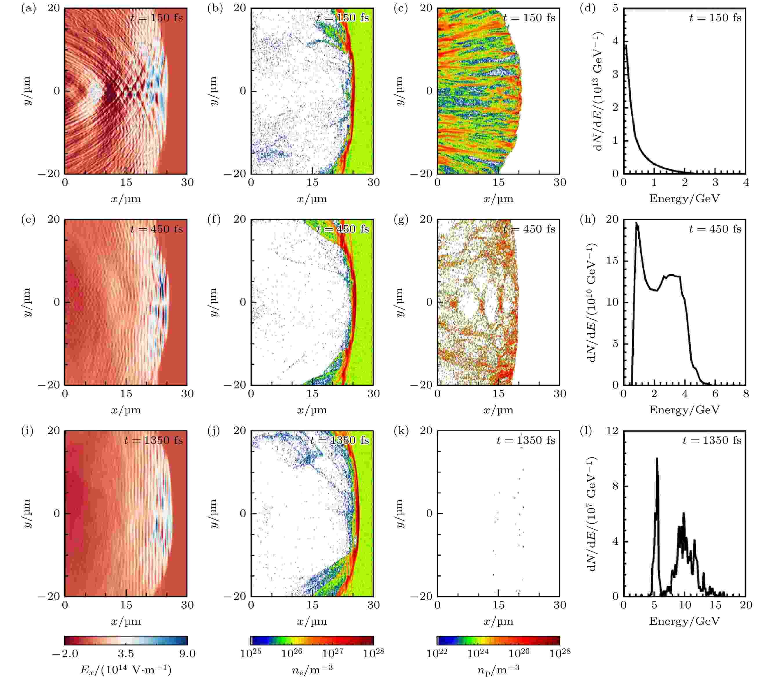
High-energy proton beams have broad application prospects in medical imaging, tumor therapy and nuclear fusion physics. Laser plasma acceleration is a new particle acceleration method with great potential because its acceleration gradient can reach 103–106times that of traditional acceleration method, so it can theoretically accelerate electrons and ions to high energies in the scale of a few centimeters to a few meters. Radiation pressure acceleration (RPA) is considered to be the most promising mechanism of high energy proton acceleration in laser plasma acceleration, but the Rayleigh-Taylor instability (RTI) inherent in the process of radiation pressure acceleration will cause transverse density modulation on the target surface, resulting in the premature termination of the proton acceleration process and the failure to obtain high energy proton beams. In order to obtain high-energy proton beams, an acceleration scheme combining radiation pressure acceleration with laser wakefield is proposed. In this scheme, a high-energy proton beam with peak energy of 22.2 GeV, cut-off energy of 36.4 GeV and charge of 0.67 nC is obtained by adding a uniform density plasma channel at the back end of the thin target with critical density, the cut-off energy of the high energy proton can be increased by two orders of magnitude compared with the proton only in the radiation pressure acceleration process. The results confirm that in a uniform-density plasma channel connected behind a thin target, the laser wakefield can capture protons pre-accelerated by the radiation pressure process and maintain the acceleration for a long period of time, finally obtain high-energy protons. The acceleration of protons in plasma channels with different uniform densities is also investigated in this work, and it is found that the higher the density, the higher the peak energy, cut-off energy and charge of the accelerated protons are. The combined acceleration scheme is instructive for the generation and application of high-energy proton beams.

2024, 73 (11): 115203.
doi:10.7498/aps.73.20240273
Abstract +
Microwave discharge neutralizer is an important part of microwave discharge ion thruster system, which plays a vital role in maintaining potential balance between spacecraft and neutralizing ion beam. Its electron extraction property directly affects the operation condition of ion thruster system. In order to break through the power limit of miniature microwave discharge ion thruster, a magnet array microwave discharge ion thruster system is designed and tested. In the experiment on finalizing magnetic field structure of magnet array microwave discharge neutralizer, an interesting phenomenon is found that theI-Vcurves of electron current, after rotating the magnetic array orientation, are very different. Defining forward direction of magnet array can normally extract electrons, then backward direction of magnet array can hardly extract electrons. Because the diameter of discharge chamber is only 10 mm, it is too small to perform Langmuir probe diagnosis. And thus, an integrative particle-in-cell method is used to simulate the neutralizer operation processes of two different magnetic field structures, and for the sake of accuracy, real vacuum permittivity is used. The simulation results show good consistence with experimental phenomenon. In the initial discharge process, it is found that the magnetic field gradient leads to different plasma distributions; in electron extraction process, it is found that the potential distribution near the orifice determines the electron extraction property of the neutralizer. Through comparing the plasma parameter distributions under different magnetic field structures and operating voltages, an assumption that the ion is an important factor in electron extraction process is proposed. Then, a simulation that ions disappear artificially outside the orifice is conducted, and the simulation results show that electrons cannot be effectively extracted without ions near the orifice. According to the simulation and experiment results, two necessary conditions are summarized for electron extraction of the neutralizer. The first condition is magnetic field structure: the magnetic field gradient should point towards the orifice to guide plasma migration towards the orifice, the second one is potential distribution: there should be enough ions to lift the potential near the orifice for reducing or breaking the potential well. These two conditions can help understand the electron extraction mechanism of microwave discharge neutralizer and provide theoretical reference for optimizing the performance of neutralizer in future.
2024, 73 (11): 115204.
doi:10.7498/aps.73.20231733
Abstract +
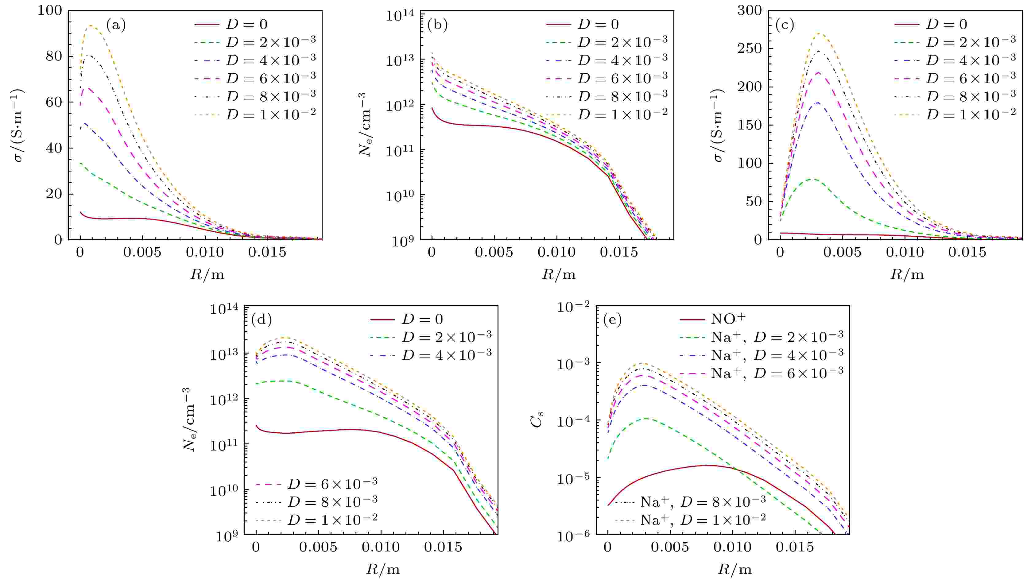
Surface ablation significantly affects the distribution of plasma in high-speed flow and the characteristics of its interaction with electromagnetic fields. Considering the mechanism of ablation and ejection on the surface of hypersonic vehicle, the participation of ablation products in the plasma generating process in the flow field, the conduction mechanism of mixed ionized gas containing alkali metal and the electromagnetic dynamics mechanism, the coupled calculation method of high-speed flow/plasma/electromagnetic field with alkali metal ablation is established by solving the three-dimensional thermochemical non-equilibrium flow governing equation with electromagnetic source term, the electric field Poisson equation and the magnetic vector Poisson equation. Combined with the common ablation and pyrolysis process of carbon-carbon materials and silicon-based phenolic resin materials, the mechanism and law of the interaction between surface ablation and electromagnetic field on the hypersonic plasma sheath under various conditions are systematically studied. The results show that the ablation effect affects the plasma distribution in the flow field, which is affected by the ablation mass ejection rate and the mass proportion of alkali metal. When the alkali metal content is high, the alkali metal ionization reaction is dominant, and the electron number density can increase by 1–2 orders of magnitude. The influences of different materials on plasma are different. The mass ejector ratio of silicon-based phenolic resin is larger, and the molar concentration of CO+and C+produced by ionization is close to that of NO+and
${\mathrm{O}}_2^+ $
, which cannot be ignored. Alkali metal in ablative material can significantly improve the control effect of magnetohydrodynamics. With the increase of the proportion of alkali metal, the coupling effect of electromagnetic field increases, and the relationship between them is nonlinear. When the speed is low, the ionization degree of air itself is low and the coupling effect of electromagnetic field is weak. But the efficiency of “improving the electromagnetic effect by ablation of alkali metal” is higher.
CONDENSED MATTER: STRUCTURAL, MECHANICAL, AND THERMAL PROPERTIES
2024, 73 (11): 116201.
doi:10.7498/aps.73.20240066
Abstract +
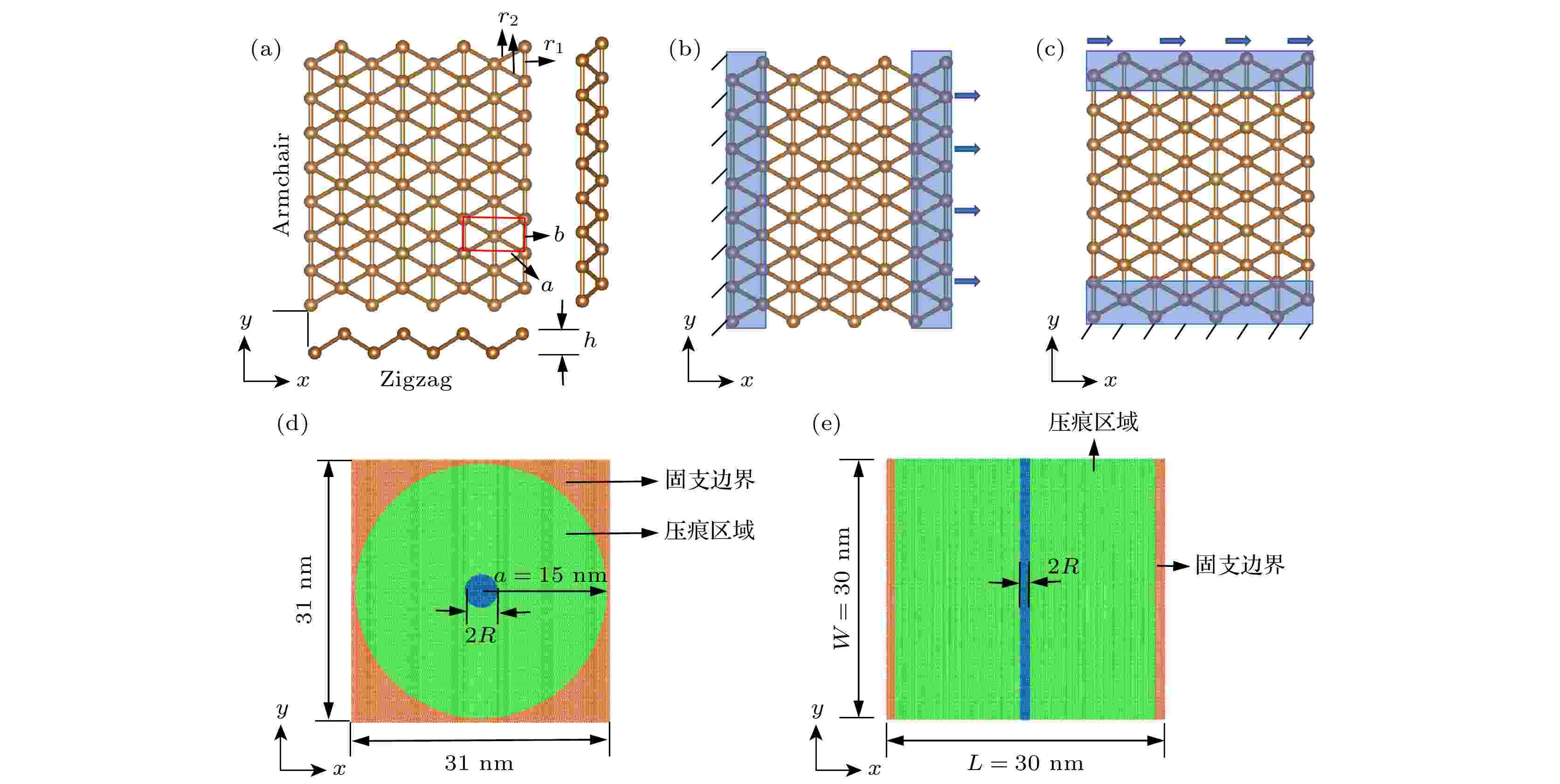
Two-dimensional (2D) borophene has attracted widespread research interest in condensed matter physics and materials science because of its rich physical and chemical properties. However, the mechanical properties and deformation mechanisms of borophene under different loadings are still unclear and not thoroughly investigated. In this work, the tensile, shear, and nanoindentation failure processes of borophene are simulated via molecular dynamics method to obtain the key mechanical parameters of borophene. The mechanical response and deformation mechanism of borophene under different loads are analyzed from the change of B—B bond length with the strain/indentation depth. The results show that the tensile mechanical properties of borophene exhibit significant anisotropic characteristics, with the Young’s modulus and strength along the armchair direction being much higher than those along the zigzag direction. However, the anisotropy of the shear mechanical properties of borophene is not significant. This phenomenon can be attributed to the different contributions of the strong B—B σ bonds and weak multi-center bonds in borophene when they are stretched in different directions. It is also found that borophene exhibits different mechanical responses under spherical indentation and cylindrical indentation. The force at failure of the borophene under spherical indentation is much lower than the value under cylindrical one, and the intrinsic mechanical parameters of borophene under spherical indentation cannot be estimated accurately because of the anisotropic characteristics of borophene. However, under cylindrical indentation, borophene exhibits similar anisotropic characteristics to those under tension, and the mechanical parameters such as Young’s modulus can be measured accurately, which are consistent with those obtained under tension. In addition, the effects of the borophene indentation model and spherical/cylindrical indenter size, the loading rate and temperature on the mechanical parameters of borophene are also studied systematically. The results indicate that the Young’s modulus of borophene from spherical indentation is highly estimated whena/R< 15 but not sensitive whena/R> 15, while the results from cylindrical indentation are hardly affected by the values ofL/RandW/L. The Young’s modulus of borophene slightly decreases with temperature increasing, while the loading rate has almost no influence on the value of Young’s modulus of borophene. These findings are expected to provide important guidelines for realizing the practical applications of borophene based micro/nano electromechanical systems.

2024, 73 (11): 116301.
doi:10.7498/aps.73.20231814
Abstract +
Presently, impurity-compensated silicon (Si) has no clear potential applications due to high resistance and few carriers. Thus, it has received little attention from researchers. In this study, we find that impurity compensation can make localized state energy levels form in Si bandgap, which can improve the light absorption of Si in the near infrared region. In this work, in order to comprehensively and deeply understand the photoelectric properties of impurity-compensated Si, the localized state energy levels composed of P+/B–ions are constructed in Si bandgap through the co-doping of phosphorus (P) and boron (B), thereby forming impurity-compensated Si. The first-principles based on a density functional theory framework is used to study the photoelectric properties of the impurity-compensated Si (n/p-Sic) such as the density of states (DOS), dielectric function and refractive index. The DOS study reveals the following results: after the n- and p-Si with the same concentration of P and B (12.5%) are fully compensated for by impurities, the Fermi energy levels of their compensated counterparts are at the valley bottom formed by the two adjacent DOS peaks, and the DOS is not zero at the valley bottom. In the study of dielectric function and refractive index, it is found that when the doping ratio isCB/CP0= 0.25, n-Sic has the largest dielectric function and refractive index in the low energy region. In addition, comparing intrinsic Si with its doped counterparts in the real part (Re) of their dielectric constant, the following regularity is found: in the high energy region ofE> 4 eV, the Re values of the intrinsic Si, n/p-Si and p-Sic are negative. In the low energy region of 0.64 eV<E< 1.50 eV, the Re value of n-Sic is negative for the doping ratio ofCB/CP0= 0.25. The above comparison indicates that the n-Sic withCB/CP0= 0.25 can achieve good metallicity in the low energy region, indicating that the electrons in valence band are easily excited by low-energy long-wavelength light. Theoretical studies show that the good photoelectric properties of n-Sic withCB/CP0= 0.25 may be related to Si dangling bonds and localized state energy levels in Si bandgap. The Si dangling bonds are caused by the impurity compensation of B dopant for n-Si, leading part of Si-Si bonds to change into Si-B bonds. This study provides theoretical guidance for the application of impurity-compensated Si in the field of photodetectors such as CMOS image sensors and infrared photodetectors.
EDITOR'S SUGGESTION
2024, 73 (11): 116401.
doi:10.7498/aps.73.20240325
Abstract +
CONDENSED MATTER: ELECTRONIC STRUCTURE, ELECTRICAL, MAGNETIC, AND OPTICAL PROPERTIES

2024, 73 (11): 117101.
doi:10.7498/aps.73.20240175
Abstract +
Antimony selenide (Sb2Se3) is a simple-phase, element-rich, and economically friendly material for solar cell absorption layers, with broad application prospects. However, the weak conductivity of Sb2Se3has become a significant factor limiting the performance of solar cell devices. Carrier mobility is an important electrical parameter for both materials and devices, and strain can change carrier mobility. Therefore, studying the effect of strain on the carrier mobility of Sb2Se3is of practical significance. In this work, using density functional theory and deformation potential theory, we systematically investigate the influence of uniaxial strain on the band structure, bandgap width, iso-surface, and effective mass of Sb2Se3. We analyze the effects of three types of uniaxial strains along thex-,y-, andz-direction on the carrier mobilities along thex-,y-, andz-direction, which are denoted byμx,μy, andμz, respectively. It is found that under these strains, the valence band maximum (VBM) position of Sb2Se3remains unchanged, and the bandgap decreases with the increase of strain along they- andz-direction, while it increases along thex-direction. The variation in bandgap may be related to the coupling strength between the Sb-5p orbital and Se-4p orbital of the conduction band minimum (CBM). For fully relaxed Sb2Se3, its iso-surface exhibits a distorted cylindrical shape, with low dispersion along thez-axis and high dispersion along thex- andy-axis, whereμxis greater thanμyandμz, suggesting that thex-direction should be considered as the specific growth direction for Sb2Se3experimentally. When the strain is applied along thex- andz-direction,μxgradually increases with strain increasing, while it decreases when the strain is applied along they-direction. Taking into account the combined effects of strain on bandgap, iso-surface, density of states, and mobility, this study suggests that the optimal performance of Sb2Se3solar cell absorber layer material can be realized when the strain is applied along they-axis, with a compressive strain of 3%.
2024, 73 (11): 117301.
doi:10.7498/aps.73.20240357
Abstract +
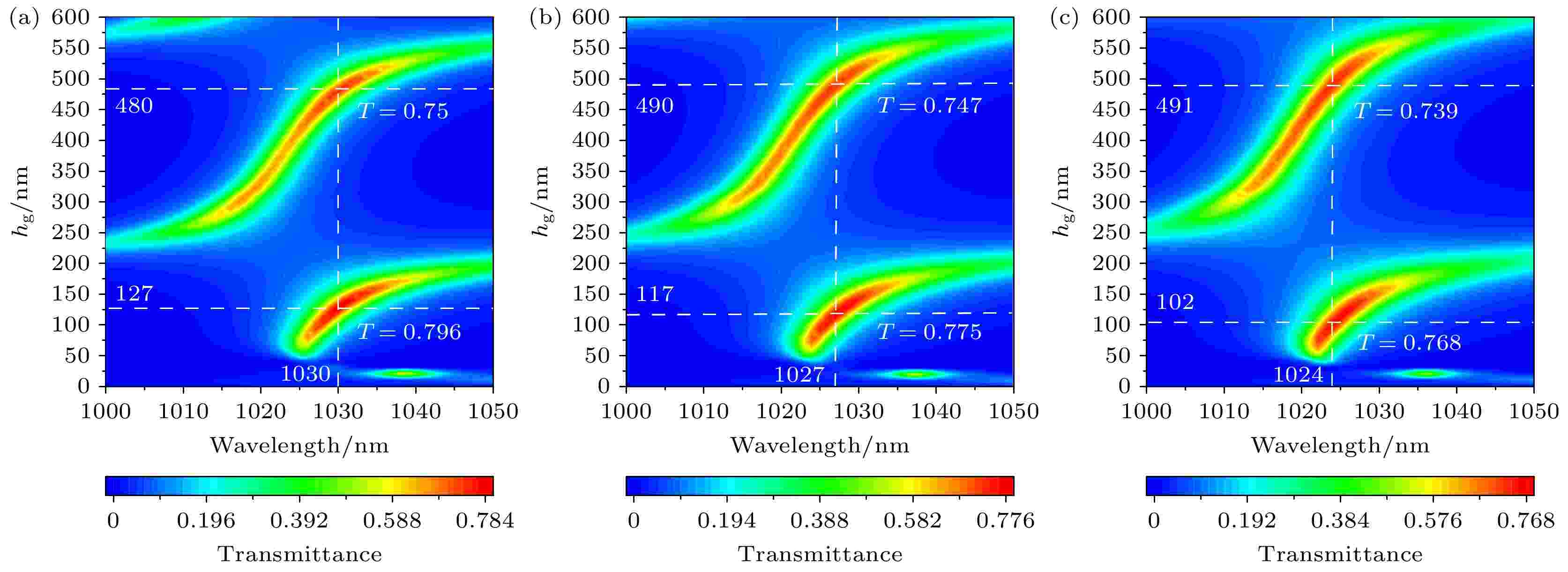
In order to observe the extraordinary optical transmission (EOT) through a metal gratings, induced by Tamm plasmon polaritons (TPPs), a layered structure consisting of a distributed Bragg reflector covered with a one-dimensional metal grating is proposed in this work. When an incident light wave passes through DBR regime and impinges on the DBR-metal interface normally, the generation of TPPs and the resulting highly localized energy on the metal-DBR interface are simulated in detail by the finite element method. As a result, the surface plasmon polariton (SPPs) modes accommodated inside the slits of metal gratings can be excited more effectively by the enhanced electromagnetic field associated with TPPs located on the interface. Furthermore, the enhanced transmission of incident light waves in the structure can be achieved when the SPP mode inside the grating slits satisfies the Fabry-Perot (FP)-like resonance condition, which reveals that the EOT in this structure comes from a TPPs-FP hybrid resonance. This inference can be confirmed by the relationships between the central wavelength and the grating height for the two transmission peaks, and the magnetic field modal profiles associated with the two peaks. Quantitative effects of the slit width and duty cycle on the transmission peak of the metal grating are analyzed numerically, and the results demonstrate that when the period is determined, as the slits width increases, the two peak transmittances first increase and then decrease. On the other hand, when the slit widths are chosen to be 40 nm, 50 nm, and 60 nm respectively, the peak transmittance first increases and then decreases with the duty cycle increasing. Meanwhile, it is found that the center wavelengths of the transmission peaks are related to the duty cycle in a nearly linear manner for three slit widths, which can be used to flexibly adjust the center wavelength of extraordinary optical transmission.
EDITOR'S SUGGESTION
2024, 73 (11): 117302.
doi:10.7498/aps.73.20240310
Abstract +
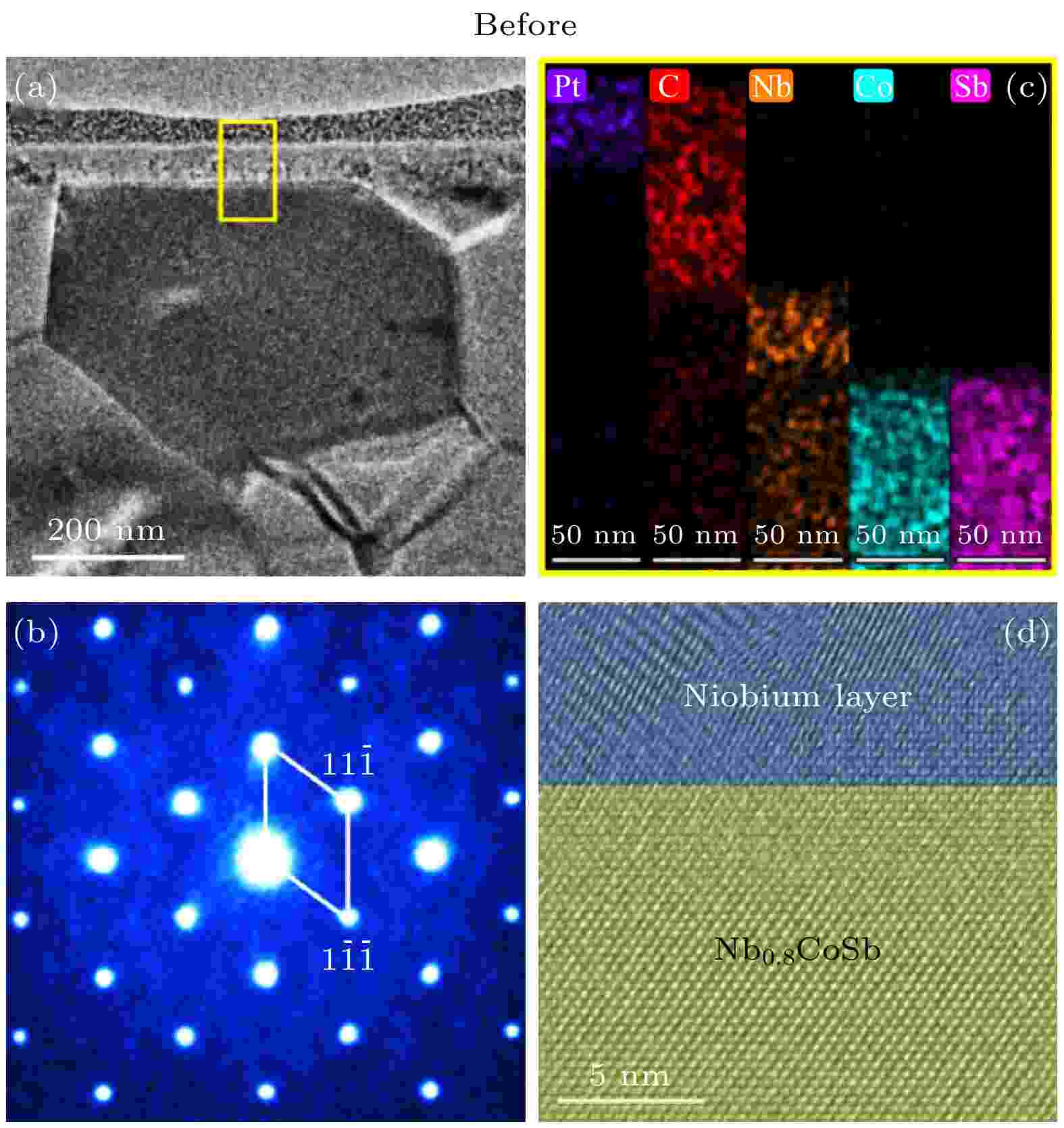
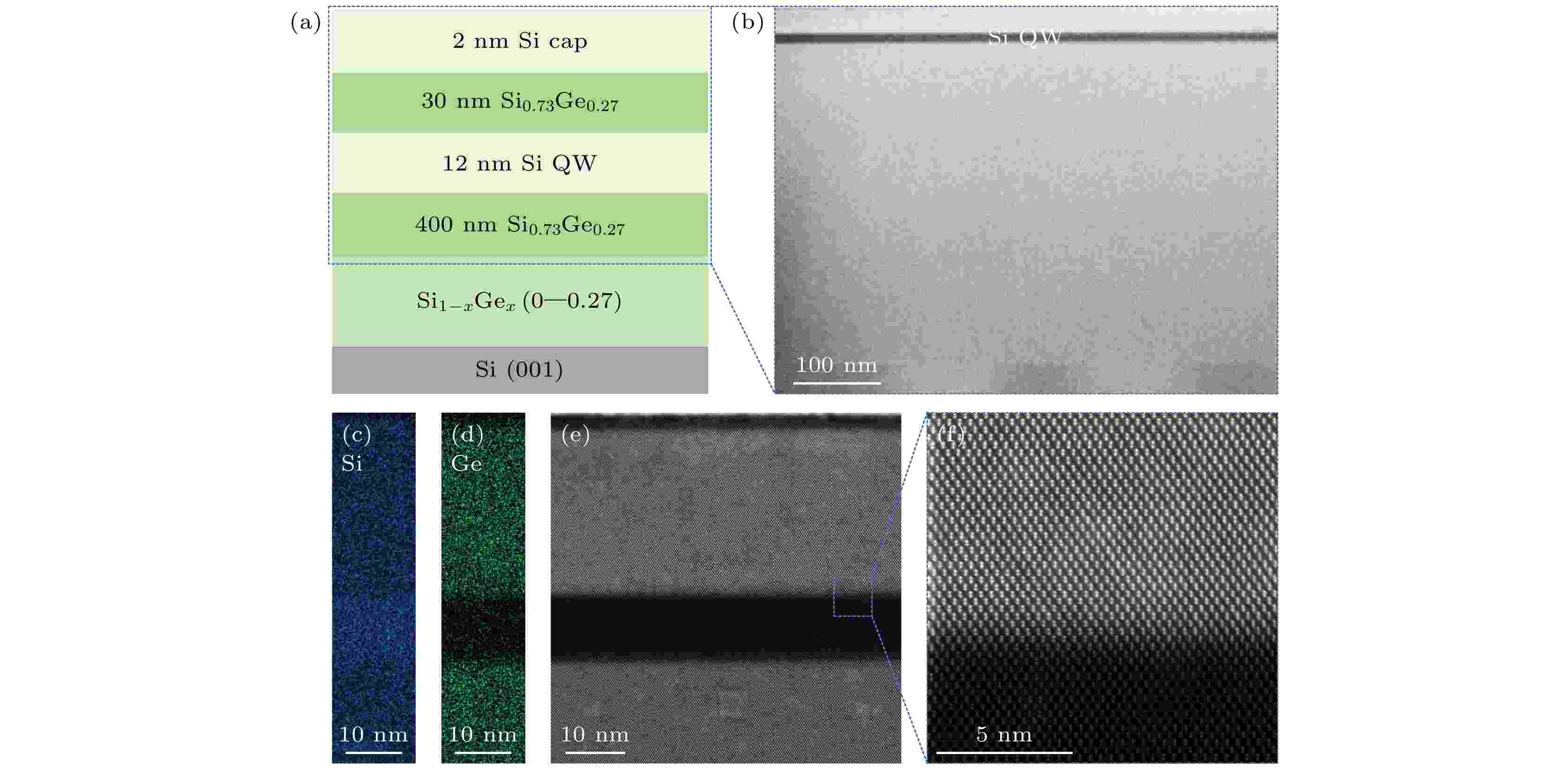
Silicon-based semiconductor quantum computing with spin as the encoding unit is compatible with traditional microelectronic processes, easy to expand, and can improve isotope purification and decoherence time, thus attracting much attention. There are fewer reports on the work related to undoped Si/SiGe heterostructures grown by molecular beam epitaxy than those on chemical vapor deposition. An undoped Si/SiGe heterostructure is grown by molecular beam epitaxy (see the attached figure below). The results from scanning transmission electron microscopy and energy-dispersive spectroscopy mapping show an atomic-scale interface with a characteristic length of 0.53 nm. The surface root-mean-square roughness measured by atomic force microscope is 0.44 nm. The X-ray diffraction data show that the Si quantum well is fully strained and the in-plane strain is 1.03%. In addition, the performance of the two-dimensional electron gas is evaluated by low-temperature Hall measurements, which are conducted in the Hall-bar shaped field-effect transistor. The peak mobility is 20.21×104cm2·V–1·s–1when the carrier density is about 6.265×1011cm–2at 250 mK. The percolation density is 1.465×1011cm–2. The effective mass of the two-dimensional electron gas is approximately 0.19m0. The power exponential between carrier density and mobility at different gate voltages is 1.026, and the Dingle ratio of the two-dimensional electron gas is in a range of 7–12, indicating that the electrons are scattered by background impurities and semiconductor/oxide interfaces charges. The atomically sharp interface of Si/SiGe heterostructures created by molecular beam epitaxy is beneficial for studying the valley physics properties in silicon. The structural and transport characterizations in this paper lay the foundation for the optimization of Si-based semiconductor quantum dot quantum computing materials.

EDITOR'S SUGGESTION
2024, 73 (11): 117701.
doi:10.7498/aps.73.20240367
Abstract +
Spintronic devices utilize the spin property of electrons for the storage, transmission, and processing of information, and they possess inherent advantages such as low power consumption and non-volatility, thus attracting widespread attention from both academia and industry. Spin-orbit torque (SOT) is an efficient method of manipulating magnetic moments through using electric current for writing, controlling the spin-orbit coupling (SOC) effect within materials to achieve the mutual conversion between charge current and spin current. Enhancing the efficiency of charge-spin conversion is a critical issue in the field of spintronics. Strontium ruthenate (SRO) in transition metal oxides (TMO) has attracted significant attention as a spin source material in SOT devices due to its large and tunable charge-to-spin conversion efficiency. However, current research on SOT control in SRO primarily focuses on utilizing substrate strain, with limited exploration of other control methods. Crystal orientation can produce various novel physical properties by affecting material symmetry and electronic structure, which is one of the important means to control the properties of TMO materials. Considering the close correlation between the SOT effect and electronic structure as well as surface states, crystal orientation is expected to affect SOT properties by adjusting the electronic band structure of TMO. This work investigates the effect of crystal orientation on the SOT performance of SrRuO3film and develops a novel approach for SOT control. The (111)-oriented SRO/CoPt heterostructures and SOT devices are prepared by using pulse laser deposition, magnetron sputtering, and micro-nano processing techniques. Through harmonic Hall voltage(HHV) measurements, we find that the SOT efficiency reaches 0.39, and the spin Hall conductivity attains 2.19×10⁵
$\hbar $
/2eΩ–1·m–1, which are 86% and 369% higher than those of the (001) orientation, respectively. Furthermore, current-driven perpendicular magnetization switching is achieved in SrRuO3(111) device at a low critical current density of 2.4×10¹⁰A/m2, which is 37% lower than that of the (001) orientation. These results demonstrate that the crystal orientation can serve as an effective approach to significantly enhancing the comprehensive performance of SrRuO3-based SOT devices, thus providing a new idea for developing high-efficiency spintronic devices.
2024, 73 (11): 117801.
doi:10.7498/aps.73.20231924
Abstract +
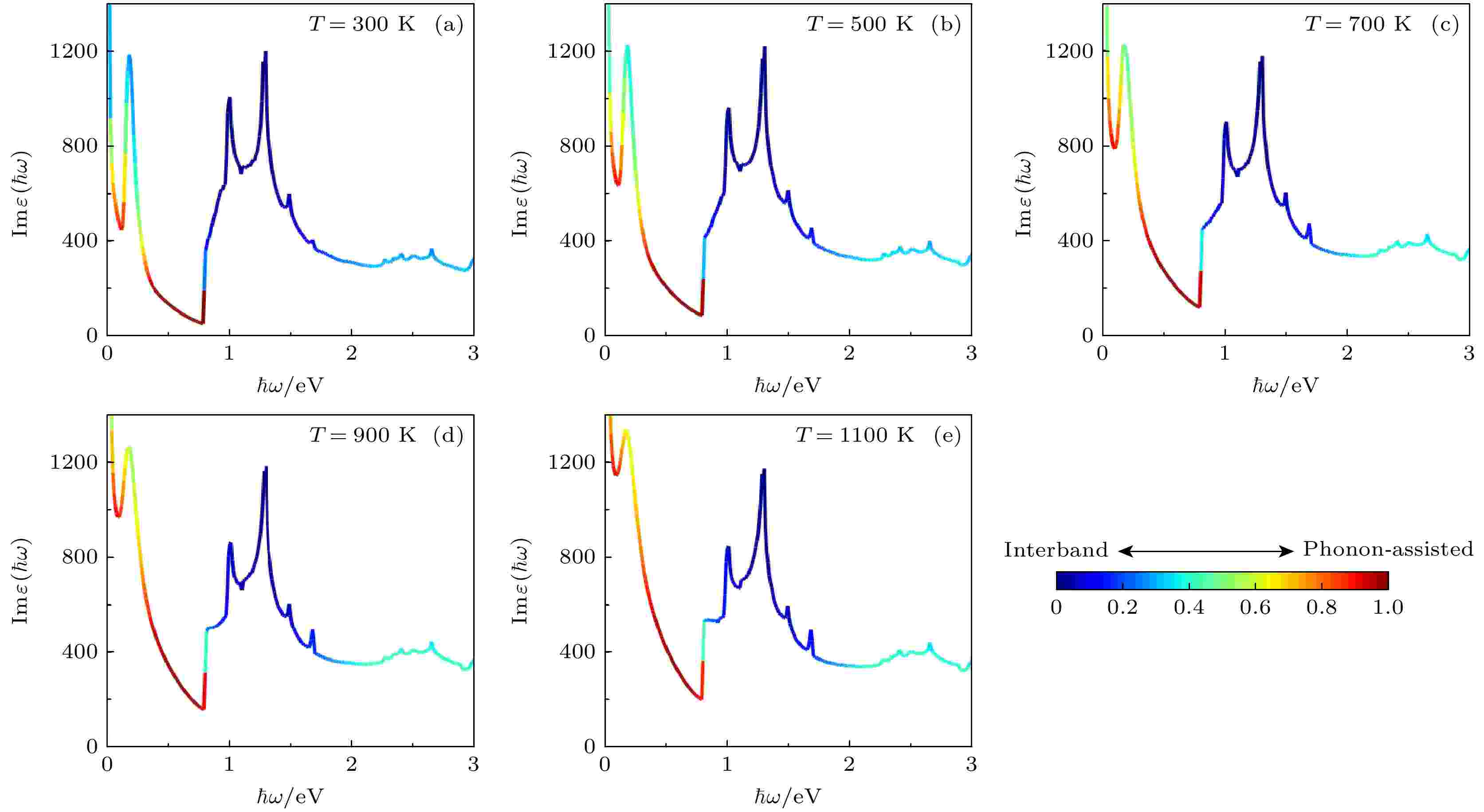
Unlike conventional optoelectronic devices, plasmon-driven optoelectronic devices can efficiently realize energy conversion and regulate the energy distribution of hot carriers through high-energy, non-equilibrium “hot” electron-hole pairs (hot carriers) generated by surface plasmon non-radiative decay, thereby presenting new opportunities for realizing hot carrier optoelectronic devices. As the basis for the practical application of plasmon optoelectronic devices, searching for plasmon metal materials with exceptional performance has always been an important topic in the field of hot carrier optoelectronic devices. Currently, MXenes can be synthesized on a large scale and has excellent photoelectric properties, so it can be used to build a variety of hot carrier photodetectors with unique structures and functions. Unlike the fixed surface ends of two-dimensional materials such as graphene, MoS2and borophene, MXenes has an abundance of surface functional groups. However, the increase of ambient temperature will accelerate the oxidation modification of surface functional groups, thus affecting the life and performance stability of optoelectronic devices. In view of the inherent limitations of experimental research on dynamic characteristics of hot carriers at continuous temperatures, we study the temperature effects on the electronic state distributions and scattering effects by using the theory of multi-body perturbation and quantum mechanics. Particularly, we introduce temperature effect into interband electron transition and phonon-assisted electron transition process to obtain temperature dependent dielectric function. From the perspective of non-radiative decay of surface plasmon, we quantify the hot carrier generation efficiency, energy distribution and transport characteristics by first principles calculations, in order to systematically study the ambient temperature dependence of plasmon-induced hot carriers in MXenes. The results show that the interband transition and the phonon-assisted electron transition in MXenes together efficiently produce high-energy hot hole-dominated carriers with a long lifetime and transport distance, which is comparable to borophene. The increase of ambient temperature significantly improves the hot carrier generation efficiency in the infrared range. Meanwhile, the physical mechanism of hot carrier generation in visible light is almost unaffected by the increase of ambient temperature, and the generated hot holes show excellent ambient temperature stability. In addition, the lifetime and transport distance of hot carriers decrease with ambient temperature increasing, which is mainly due to the enhanced scattering of electrons and optical phonons. The research results will provide theoretical and data support for quantitatively evaluating the ambient temperature stability of MXenes plasmon optoelectronic devices in practical environment.
INTERDISCIPLINARY PHYSICS AND RELATED AREAS OF SCIENCE AND TECHNOLOGY
2024, 73 (11): 118101.
doi:10.7498/aps.73.20240362
Abstract +
EDITOR'S SUGGESTION
2024, 73 (11): 118201.
doi:10.7498/aps.73.20240134
Abstract +
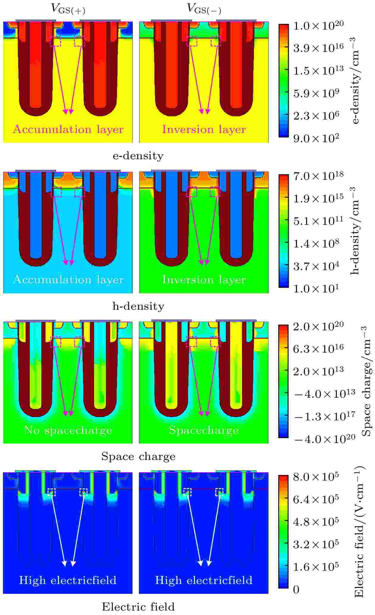
2024, 73 (11): 118501.
doi:10.7498/aps.73.20240144
Abstract +
In the actual human body model (HBM) test, it is found that the electrostatic discharge (ESD) test results of various power metal-oxide-semiconductor field-effect transistor (MOSFET) devices show asymmetry between forward withstand voltage and reverse withstand voltage, while the ESD process does not distinguish between positive direction and negative direction. Large differences between forward and reverse withstand voltages are unacceptable for power MOSFETs or as ESD protection devices. The problem of its causing device failure is particularly pronounced. In this work, by establishing the analytical model of gate-to-source capacitance of SGT-MOSFET, VUMOSFET and VDMOS under the forward and reverse voltages, we comparatively analyze the reasons for the asymmetry of the forward and reverse withstand voltages and their different ratios of the three kinds of power MOSFETs, which provides a theoretical basis for testing the device’s ESD and the analyzing their reliability. It is found that the ESD forward and reverse withstand voltage asymmetry phenomena of different power MOSFET structures are related to the variation of gate-to-source capacitance, caused by the reverse-type layer. When a forward voltage is applied across the gate and source, the device gate-to-source capacitance consists of the oxide layer capacitance around the gate in parallel; when a reverse voltage is applied, the gate-to-source capacitance consists of the virtual gate-to-drain capacitance in series with the inverse layer capacitance and then in parallel with the other oxide layer capacitance around the gate. This results in a decrease of the gate-to-source capacitance at the reverse voltage, making the device reverse withstand voltage greater than the forward withstand voltage. The difference in the ratio of ESD reverse withstand voltage to forward withstand voltage among different devices is related to the change of the capacitance of the inverse layer in the gate-to-source capacitor under reverse voltage caused by the difference in device structure.
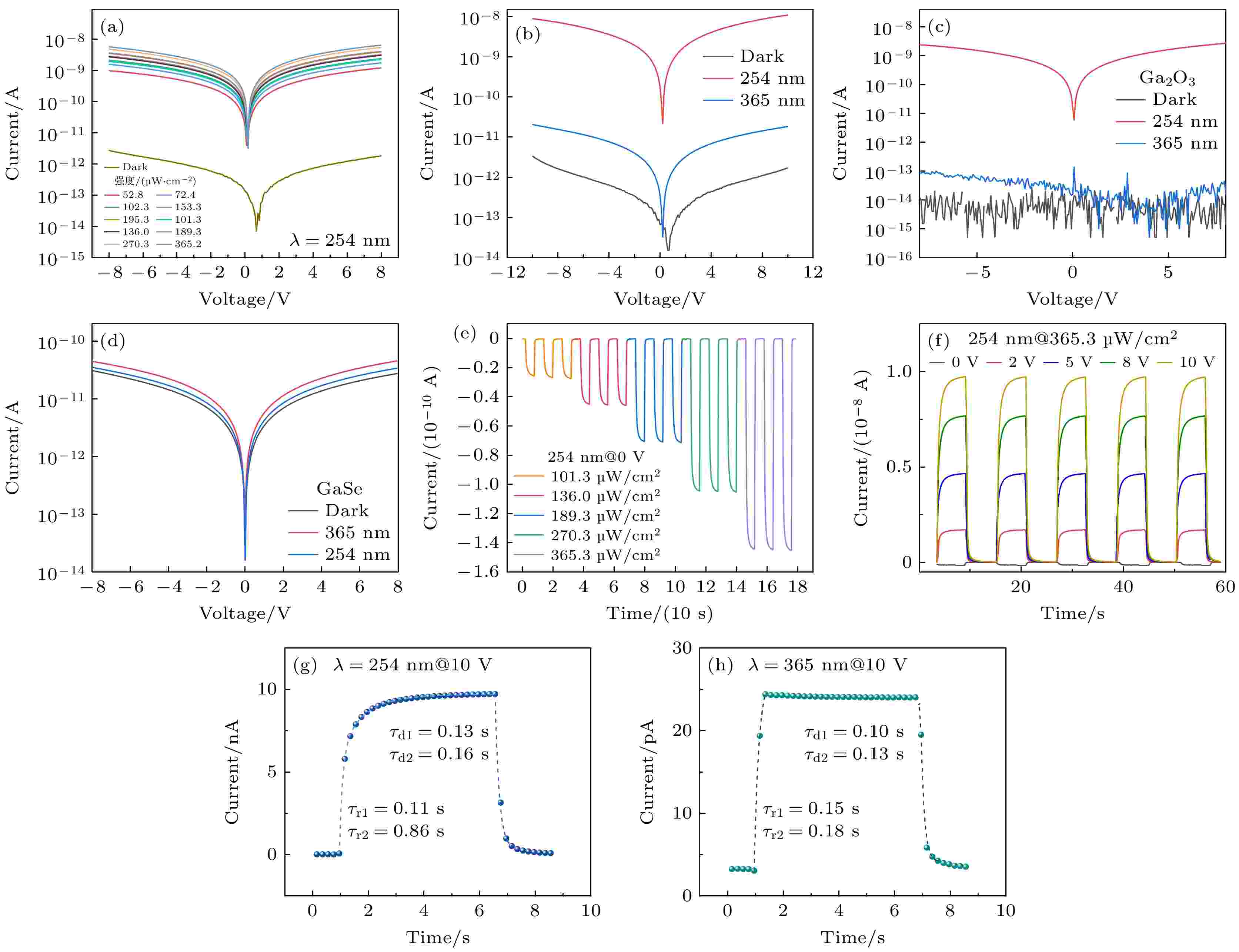
2024, 73 (11): 118502.
doi:10.7498/aps.73.20240267
Abstract +
UV photodetectors have the advantages of high sensitivity and fast response speed. As an ultra-wide bandgap semiconductor, gallium oxide (Ga2O3) plays an extremely important role in detecting deep ultraviolet. It can form a typical type-II heterostructure with GaSe, promoting carrier separation and transport. In this work, Ga2O3epitaxial films are grown on sapphire substrates by plasma-assisted chemical vapor deposition (PECVD). The GaSe films and GaSe/β-Ga2O3heterojunction photodetectors are grown on gallium oxide films by Bridgeman technology. The detector has a good response to deep ultraviolet light, the dark current of the device is only 1.83 pA at 8 V, and the photocurrent reaches 6.5 nA at 254 nm. The UVC/Visible (254 nm/600 nm) has a high rejection ratio of about 354. At very small light intensities, the responsivity and detection can reach 1.49 mA/W and 6.65 × 10¹¹Jones, respectively. At the same time, due to the photovoltaic effect formed by the space charge region at the junction interface, the detector exhibits self-powered supply performance at zero bias voltage, and the open-circuit voltage is 0.2 V. In addition, the detector has a very good sensitivity. The device can respond quickly, whether it is irradiated with different light intensities under constant voltage, or with different voltages under constant light intensity. It can respond within milliseconds under a bias voltage of 10 V. This work demonstrates the enormous potential of heterojunctions in photoelectric detection by analyzing the photophysical and interface physical issues involved in heterojunction photodetectors, and provides a possibility for detecting the deep ultraviolet of gallium oxide.
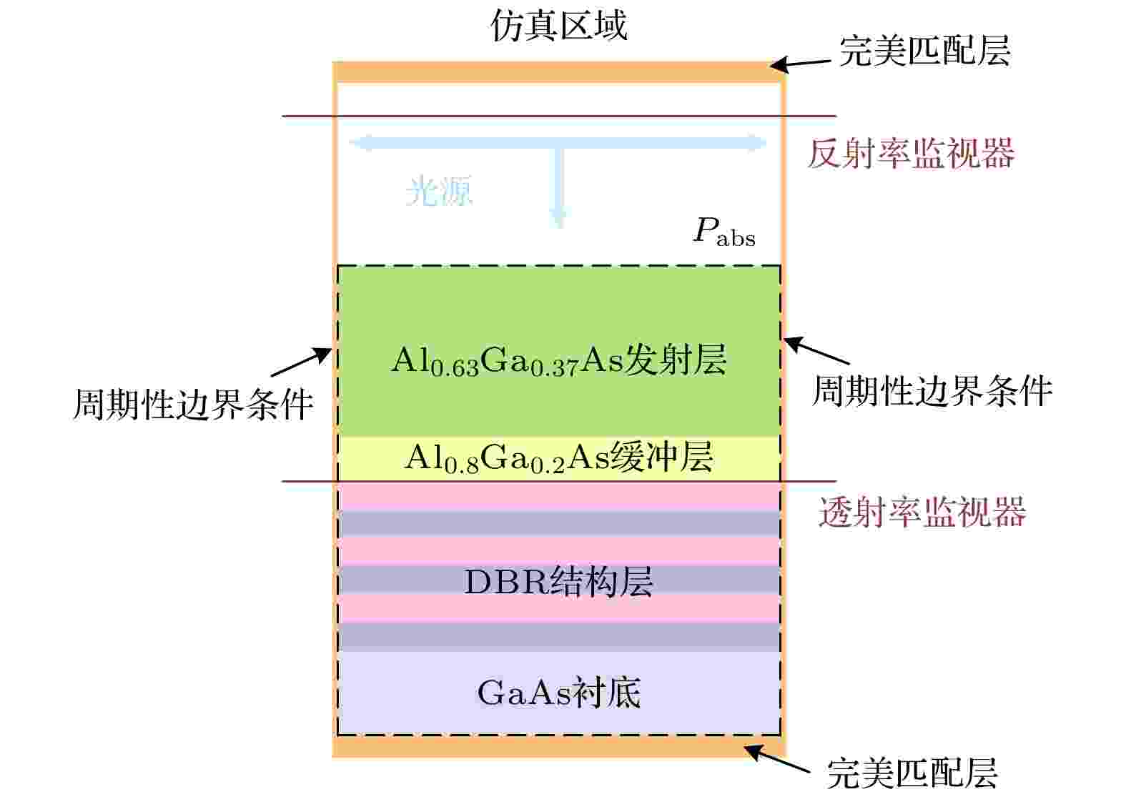
2024, 73 (11): 118503.
doi:10.7498/aps.73.20240253
Abstract +
The AlGaAs photocathode can be used in the field of underwater optical communication because of its fast response speed and adjustable spectral response range. In order to solve the problem that the low light absorption of the AlGaAs emission layer limits the improvement of its quantum efficiency, the distributed Bragg reflector (DBR) structure is used to reflect the light at a specific wavelength back to the emission layer to further increase the absorption rate, thus improving the response capability of the photocathode at 532 nm. The spectral response model of the AlGaAs photocathode with DBR structure is obtained by solving one-dimensional continuity equation. The optical model of the AlGaAs photocathode with enhanced response at 532 nm is established by the finite-difference time-domain method. The effects of the sublayer periodic pairs, the sublayer material and the thickness of emission layer and buffer layer on the absorption rate of emission layer are analyzed. The light absorption distributions of AlGaAs photocathode with and without DBR structure are compared, and the influence mechanism of DBR structure on the blue-green light absorption capacity of AlGaAs photocathode emission layer is clarified, which can provide a theoretical basis for designing its structural parameters. The results show that the DBR structure with a periodic pair of 20 and Al0.7Ga0.3As/AlAs has the best reflection effect on 532 nm light. Based on the DBR structure, when the thickness of the emission layer and buffer layer are 495 nm and 50 nm, respectively, the emission layer has the best absorption rate of 532 nm light. Furthermore, two kinds of AlGaAs photocathodes with and without DBR structure are prepared by the metal-organic chemical vapor deposition technology, and the reflectivity and profile structure of the grown samples are characterized. Then the Cs/O activation experiments are performed to compare the spectral response curves. It is found that the spectral response of the AlGaAs photocathode sample with DBR structure at 532 nm wavelength is about twice that of the sample without DBR structure.
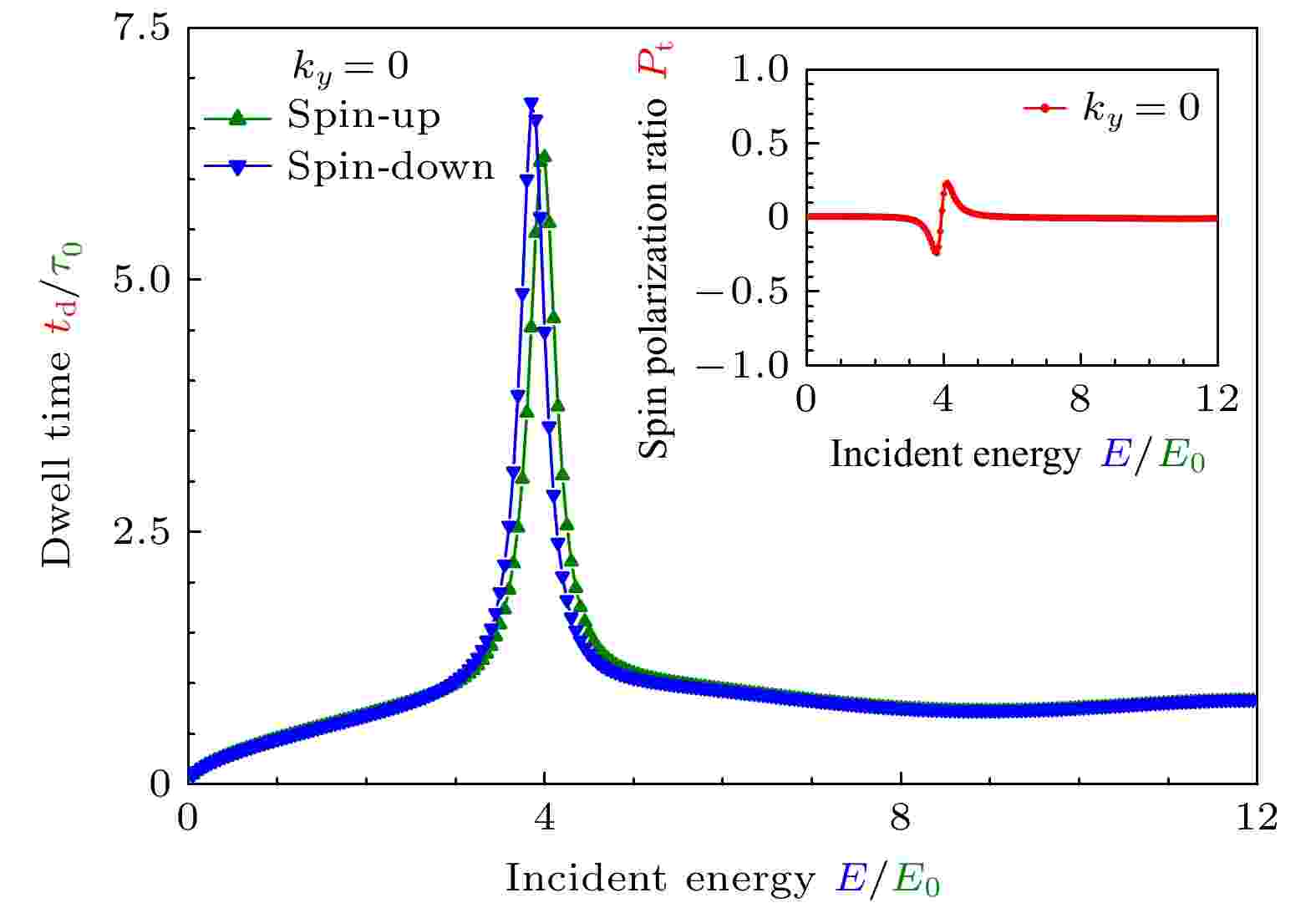
2024, 73 (11): 118504.
doi:10.7498/aps.73.20240285
Abstract +
Because digital information in semiconductor spintronics is encoded, stored, processed, and transferred by electron spins instead of its charge, the operation of a spintronic device requires that electrons in semiconductors be spin polarized. But spin states of electrons in traditional semiconductor materials are usually degenerate, therefore, conventional semiconductors cannot be directly used to design spintronic devices. Thus, how to spin polarized electrons in ordinary semiconductors (also called spin injection) including its effective manipulation, has become an important direction of research. In physics, either Zeeman effect between electron spins and external magnetic fields or spin-orbit coupling of electron spins and its spatial momentums can be employed to achieve electron-spin polarization. According to these physical mechanisms, some effective schemes have been developed successfully, such as spin filtering, temporally separating electron-spins, and spatial separations of electron spins. Utilizing the combination of theoretical analysis and numerical calculation, transmission time is investigated by considering both Zeeman effect as well as Rashba and Dresselhaus spin-orbit couplings for electron in magnetically confined semiconductor nanostructure, which is constructed on the GaAs/AlxGa1–xAs heterostructure. Schrödinger equation of an electron is numerically solved by matrix diagonalization and improved transfer-matrix method. Adopting H.G. Winful’s theory, dwell time of electron is calculated and spin polarization ratio is given. Due to Zeeman effect and spin-orbit coupling, dwell time of electron is obviously associated with the spins, which is used to separate electron-spins in time dimension and to realize spin polarization of electrons in semiconductors. Because the semiconductor GaAs has a small effective g-factor, which is about 4 times larger than that induced by Zeeman effect, electron-spin polarization originates mainly from spin-orbit coupling including Rashba and Dresselhaus types. Dwell time of electron and its spin polarization can be efficaciously modified by interfacial confining electric-field or strain engineering, because the effective potential of electron is related to spin-orbit coupling’s strength. These interesting findings not only have some references for spin injection into semiconductors, but also provide a controllable temporal electron-spin splitter for semiconductor spintronics device applications.
GEOPHYSICS, ASTRONOMY, AND ASTROPHYSICS

EDITOR'S SUGGESTION
2024, 73 (11): 119601.
doi:10.7498/aps.73.20240229
Abstract +
Due to the ability of exciton-polariton condensates formed in semiconductor microcavities to be achieved at room temperature and their characteristics such as non-equilibrium and strong interactions, they have become an ideal platform for studying the nonlinear properties of non-equilibrium quantum systems. In 2013, the research group led by L. Dominici observed two-dimensional symmetric shock waves in the polariton condensate driven by coherent pump. However, owing to the characteristics of this system, theoretical researches have lagged behind. In one-dimensional polariton condensates, disregarding cross-interaction of the system, a type of asymmetric shock wave was respectively discovered by A. M. Kamchatnov in 2012 and A. M. Belounis in 2017. In 2023, utilizing the adiabatic approximation, our research team not only uncovered sparse wave, symmetric, and asymmetric shock waves in the system, but also revealed that the symmetric shock waves are triggered by cross-interaction. At present, there is no theoretical research on shock waves in two-dimensional polariton condensate. In this paper, spectral methods and fourth-order Runge-Kutta methods are used to explore the generation and control of shock waves in two-dimensional polariton condensates. It is found that when the cross-interaction between the condensate and the polariton thermal reservoir is quenched at high condensation rates, the initially prepared bright solitons can be modulated into two types of rotationally symmetric shock waves with different velocities, while the initial dark-like solitons can only transform into a single velocity rotationally symmetric shock wave. If quenching the external potential, the dark-like solitons can be transformed into anisotropic supersonic shock waves, and the dependence of shock wave on the width of the external potential is also shown. When the external potential and incoherent pumping are controlled at low condensation rates, multiple anisotropic shock waves can be excited in a uniform condensate, and their amplitudes can be used to control the wave number and amplitude of the shock waves and the range of widths for the external potential or incoherent pumping to excite shock waves is also demonstrated. The proposed methods in this paper not only provide theoretical guidance for the generation and control of shock waves in exciton-polariton condensates, but also find symmetric shock waves similar to experiments (
Nat. Commun.
6, 8993
) without adopting any approximation, and open up a universal pathway for exciting shock waves in non-equilibrium or non-integrable systems, which may become a paradigm for transforming solitons into shock waves and significantly propel the rapid development of shock wave theory in different domains.


