GENERAL
EDITOR'S SUGGESTION
2022, 71 (6): 060702.
doi:10.7498/aps.71.20211853
Abstract +
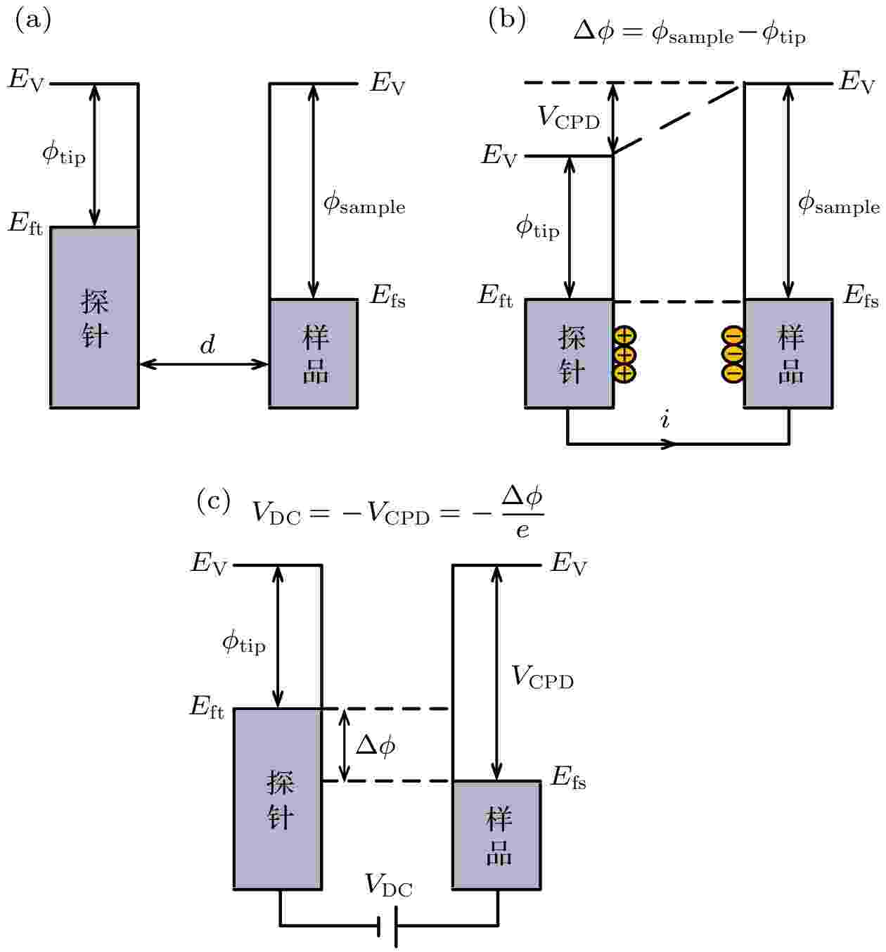
The structural properties and local contact potential difference of Au on Si(111)-(7×7) surface are studied by the homemade ultra-high vacuum non-contact Kelvin probe force microscope. Although scanning tunneling microscopy has been widely used to study the metal- adsorbed semiconductor surfaces on an atomic scale, the tunnel current measured by scanning tunneling microscopy is easy to lead the charge states to accidentally switch in the measurement process, and it is limited only to the observation of metal and semiconductor surfaces. Kelvin probe force microscope allows us to directly measure the charges at different positions of various flat surfaces by local contact potential difference on an atomic scale, which has become a more convenient and accurate means of charge characterization. In this paper, the topography and local contact potential difference of Au adsorbed Si(111)-(7×7) surface are measured on an atomic scale by Kelvin probe force microscope at room temperature, and the corresponding adsorption model and first principle calculation are established. The differential charge density distribution of the stable adsorption position of Au/Si(111)-(7×7) is obtained, and the local contact potential energy difference relationship of the stable adsorption position of Au on Si surface is given, The mechanism of charge transfer between Au atom and Si(111)-(7×7) surface during adsorption is analyzed. The experimental results show that at room temperature, single Au atom will form triangular delocalized adsorption state in the half unit cell of Si(111)-(7×7). The delocalized adsorption state is due to the fact that the moving speed of a single Au atom in the HUC is faster than the scanning speed of Kelvin probe force microscope, and the local contact potential difference measurement of Au/Si(111)-(7×7) adsorbed surface can effectively identify Au and Si atoms. Obviously, this research is of great significance in promoting the development of surface charge precision measurement, and is expected to provide some insights into the charge properties of metal adsorbed semiconductor surfaces.
EDITOR'S SUGGESTION
2022, 71 (6): 060202.
doi:10.7498/aps.71.20211625
Abstract +
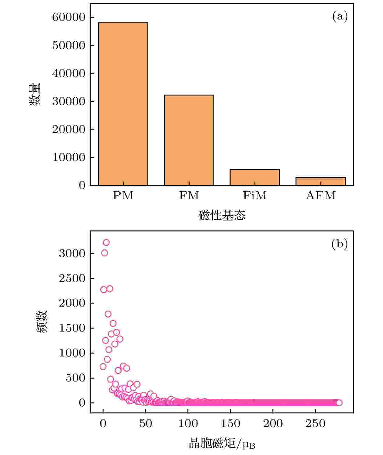
Magnetic materials are important basic materials in the information age. Different magnetic ground states are the prerequisite for the wide application of magnetic materials, among which the ferromagnetic ground state is a key requirement for future high-performance magnetic materials. In this paper, machine learning is used to study the classification of ferromagnetic, antiferromagnetic, ferrimagnetic and paramagnetic ground states of inorganic magnetic materials and the prediction of magnetic moments of inorganic ferromagnetic materials. We obtain 98888 inorganic magnetic materials data from the Materials Project database, containing material ids, chemical formulae, CIF files, magnetic ground states and magnetic moments, and extract 582 elemental and structural features for the inorganic magnetic materials by using Matminer. We design a two-step feature selection method. In the first step, RFECV is used to evaluate material features one by one to remove redundant features without degrading the model accuracy. In the second step, we rank the material features to further refine and select the most important material features for the model, and 20 material features are selected for the classification of magnetic ground states and the prediction of magnetic moments, respectively. Among the selected material features, it is found that the electronegativity, the atomic own magnetic moment and the number of unfilled electrons in the atomic peripheral orbitals all make important contributions to the classification of magnetic ground states and the prediction of magnetic moments. We build a magnetic ground state classification model and a magnetic moment prediction model by using the random forest, and quantitatively evaluate the machine learning models by using the 10-fold cross-validation approach, and the results show that the constructed machine learning models has sufficient accuracy and generalization capability. In the test set, the magnetic ground state classification model has an accuracy of 85.23%, a precision of 85.18%, a recall of 85.04%, and an F1 score of 85.24%; the magnetic moment prediction model has a goodness-of-fit of 91.58% and an average absolute error of 0.098 μBper atom. This study provides a new method and choice for high-throughput classification and screening of magnetic ground states of inorganic magnetic materials and predicting the magnetic moment of ferromagnetic materials.
2022, 71 (6): 060301.
doi:10.7498/aps.71.20211733
Abstract +
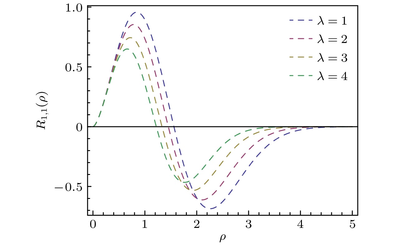
In this paper, the generalized Klein-Gordon oscillator is studied in the framework of Lorentz symmetry violation, and the Nikiforov-Uvarov method is used to analyze the Klein-Gordon oscillator with and without magnetic field. On this basis, we analyze some special cases of Klein-Gordon oscillators with Cornell potential functions in detail. The results show that the wave function and the energy eigenvalues of the generalized Klein-Gordon oscillator obviously depend on the Lorentz symmetry violation effect, and the Cornell potential function also has a non-negligible effect on the Klein-Gordon oscillator.
ATOMIC AND MOLECULAR PHYSICS
2022, 71 (6): 063201.
doi:10.7498/aps.71.20211905
Abstract +
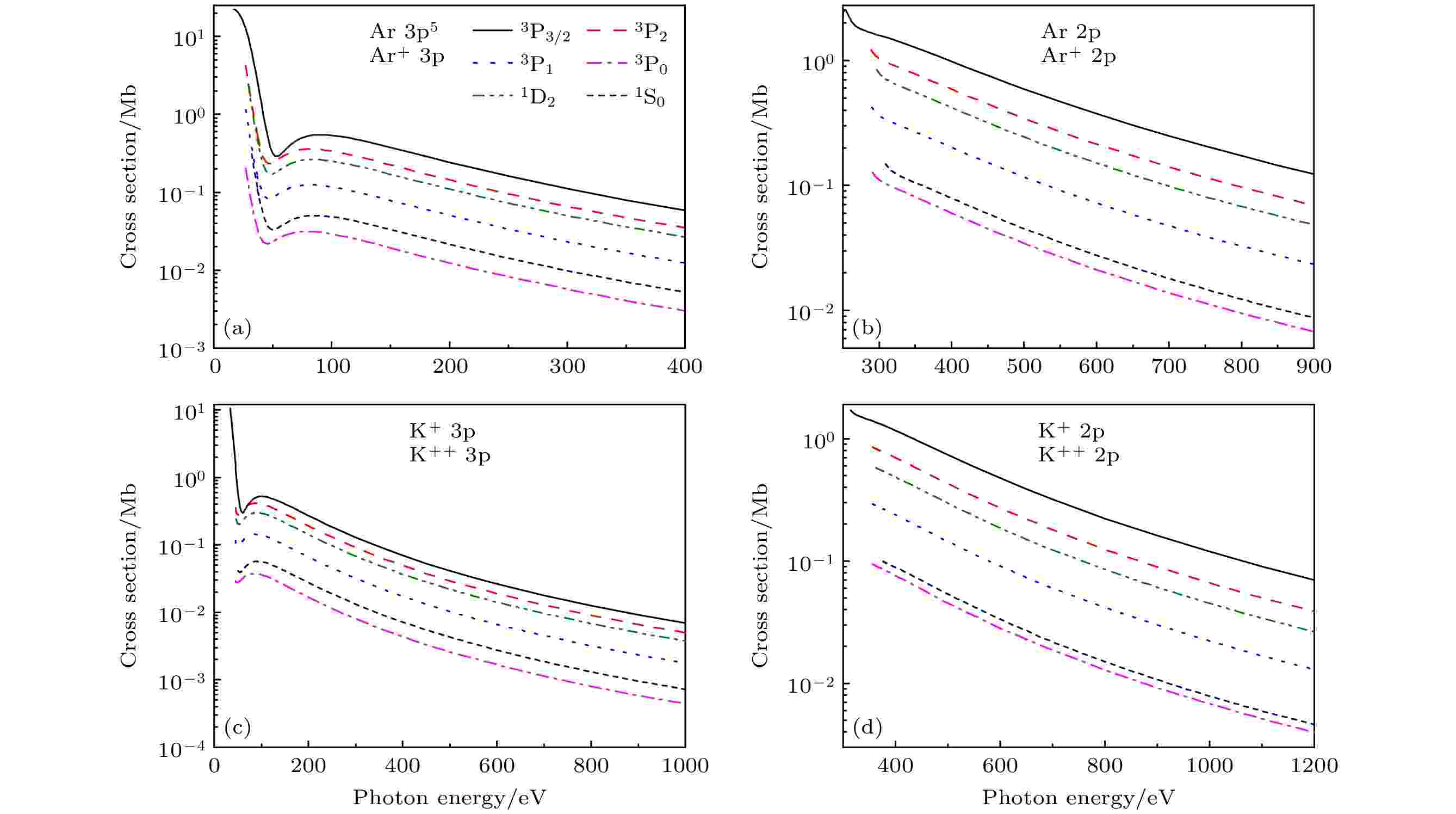
Owing to the development of XUV and X ray of the free-electron lasers, the photoelectron angular distribution in the sequential two-photon double ionization has received increasing attention of theorists and experimentalists, because it provides the valuable information about the electronic structure of atom or molecule systems and allows the obtaining of additional information about mechanisms and pathways of the two-photon double ionization. In this paper, the expression of the sequential two-photon double ionization process of the photoelectron angular distributions, including the non-dipole effects, is obtained based on the multi-configuration Dirac-Fock method and the density matrix theory, and the corresponding calculation code is also developed. Based on the code, the sequential two-photon double ionization process of the 3p and 2p shells of Ar atom and K+ion are studied, in which, the dipole and the non-dipole parameters of photoelectron angular distribution are investigated systematically. It is found that the angular distributions of the first- and second-step electrons in sequential two-photon double ionization are similar and the two photoionization processes affect each other. Near the ionization threshold, the photoionization cross-sections and anisotropy parameters for the 3p shell and the 2p shell show a large difference. While away from the threshold, the cross-section and angular anisotropy parameters of the 3p and 2p shells show similar behaviors. At the position of Cooper minimum of the photoionization cross section, the contribution of the electric dipole is suppressed, and the non-dipole effect is obvious. The non-dipole effect leads to a forward-backward asymmetric distribution of photoelectrons relative to the direction of incident light. The results of this paper will be helpful in studying the nonlinear processes of photon and matter interaction in the XUV range.
INVITED REVIEW
INVITED REVIEW
2022, 71 (6): 068503.
doi:10.7498/aps.71.20212076
Abstract +
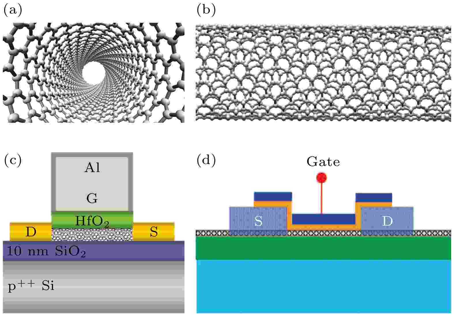
In the past 60 years, silicon-based semiconductor technology has triggered off the profound change of our information society, but it is also gradually approaching to the physical limit and engineering limit as well. Thus, the global semiconductor industry has entered into the post-Moore era. Carbon nanotube has many excellent electronic properties such as high mobility and ultra-thin body, so it has become a hopeful candidate for the new semiconductor material in the post-Moore era. After more than 20 years of development, carbon based electronic technology has made fundamental breakthroughs in many basic problems such as material preparation, Ohmic metal-semiconductor contact and gate engineering. In principle, there is no insurmountable obstacle in its industrialization process now. Therefore, in this paper the intrinsic advantages of carbon based electronic technology in the post-Moore era is introduced, the basic problems, progress and optimization direction of carbon based electronic technology are summarized, the application prospects in the fields of digital circuits, radio frequency electronics, sensing and detection, three-dimensional integration and chips for special applications are presented. Finally, the comprehensive challenges to the industrialization of carbon based electronic technology are analyzed, and its future development is also prospected.
SPECIAL TOPIC—Manipulation and applications of solid-state single quantum systems
2022, 71 (6): 060201.
doi:10.7498/aps.71.20211970
Abstract +
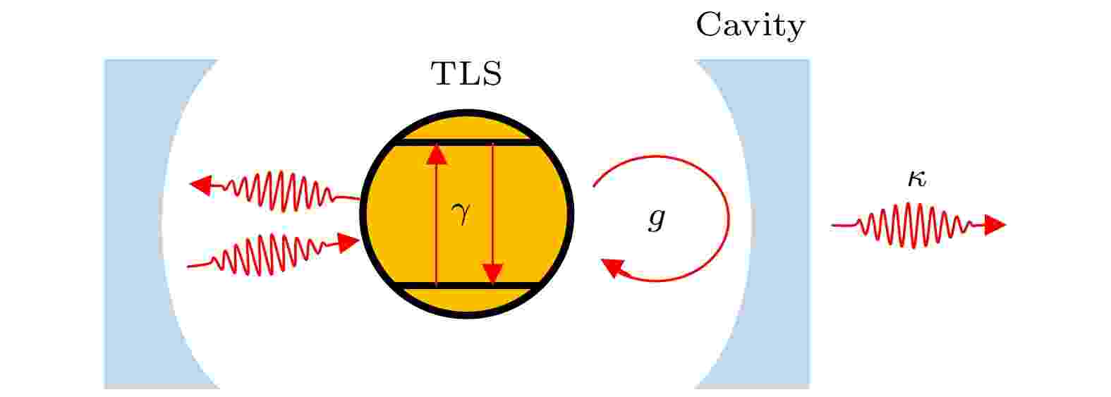
The interaction between light and matter has attracted much attention not only for fundamental research but also for applications. The open Fabry-Perot cavity provides an excellent platform for such a study due to strong optical confinement, spectral and spatial and tunability, and the feasibility of optical fiber integration. In this review, first, the basic properties of open Fabry-Perot cavities and the fabrication techniques are introduced. Then recent progress of weak coupling, strong coupling and bad emitter regimes is discussed. Finally, the challenges to and perspectives in this respect are presented.
2022, 71 (6): 060302.
doi:10.7498/aps.71.20211822
Abstract +
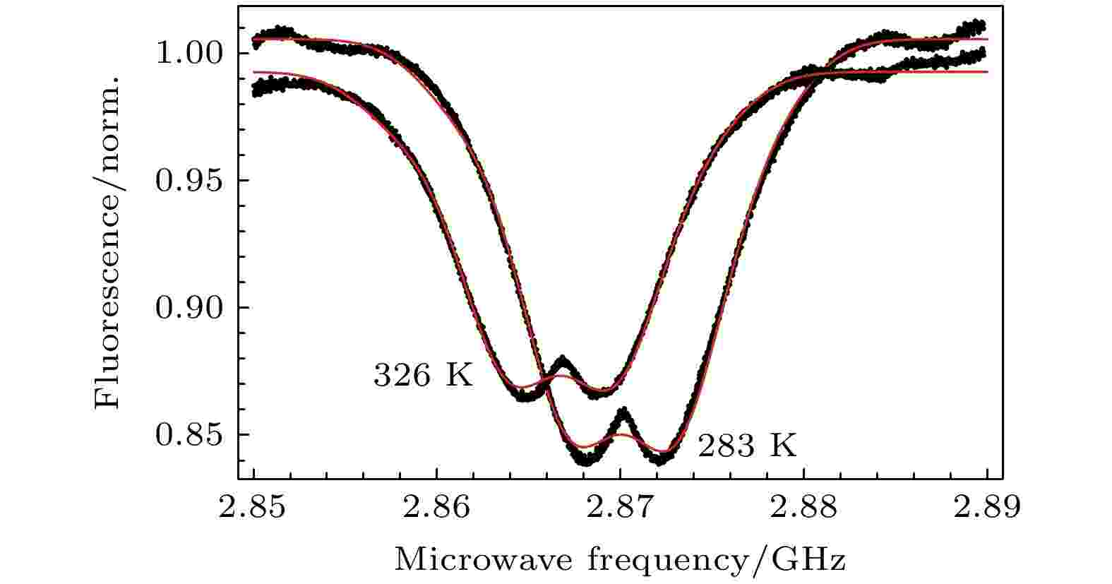
Temperature is the most intuitive and widespread in various physical quantities. Violent changes in temperature usually implies the appearing of fluctuations in physical properties of an object. Therefore, temperature is often an important indicator. With the development of science and technology, the scales in many fields are being more and more miniaturized. However, there are no mature temperature measurement systems in the case where the spatial scale is less than 10 μm. In addition to the requirement for spatial resolution, the sensor ought to exert no dramatic influence on the object to be measured. The nitrogen vacancy (NV) center in diamond is a stable luminescence defect. The measurements of its spectrum and spin state can be used to obtain the information about physical quantities near the color center, such as temperature and electro-magnetic field. Owing to its stable chemical properties and high thermal conductivity, the NV center can be applied to the noninvasive detection for nano-scale researches. It can also be used in the life field because it is non-toxic to cells. Moreover, combined with different techniques, such as optical fiber, scanning thermal microscopy, NV center can be used to measure the local temperatures in different scenarios. This review focuses on the temperature properties, the method of measuring temperature, and relevant applications of NV centers.
2022, 71 (6): 060304.
doi:10.7498/aps.71.20211808
Abstract +
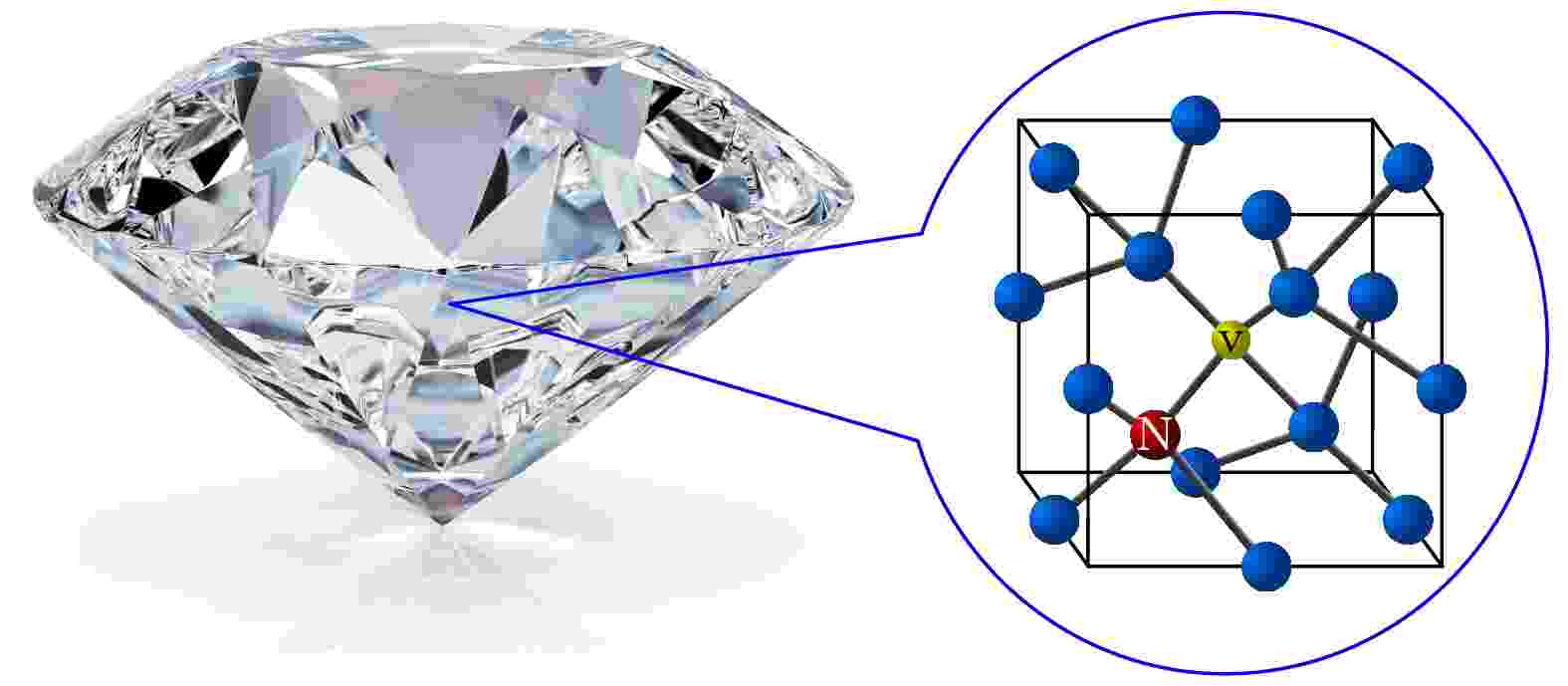
In the field of quantum physics, quantum control is essential. Precise and efficient quantum control is a prerequisite for the experimental research using quantum systems, and it is also the basis for applications such as in quantum computing and quantum sensing. As a solid-state spin system, the nitrogen-vacancy (NV) center in diamond has a long coherence time at room temperature. It can be initialized and read out by optical methods, and can achieve universal quantum control through the microwave field and radio frequency fields. It is an excellent experimental platform for studying quantum physics. In this review, we introduce the recent results of quantum control in NV center and discuss the following parts: 1) the physical properties of the NV center and the realization method of quantum control, 2) the decoherence mechanism of the NV center spin qubit, and 3) the application of single-spin quantum control and relevant research progress.
2022, 71 (6): 060701.
doi:10.7498/aps.71.20212324
Abstract +
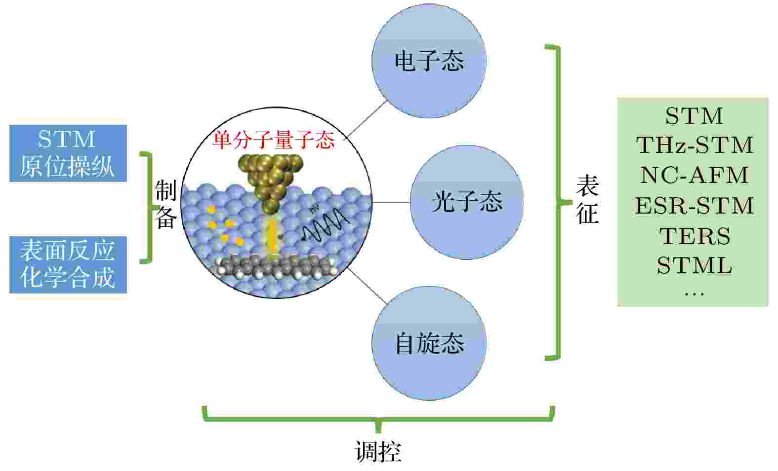
Single molecular systems are typical quantum confinement systems, which have rich electronic states, photon states and spin states due to their discrete energy levels, localized orbitals and diverse chemical structures. The states determined by quantum mechanics in these molecular systems make it possible to serve as great physical entities for future quantum information technology. The detection and manipulation of quantum states on a single molecule scale are beneficial to the bottom-up construction of quantum devices. Owing to the highly limited spatial localization of single molecular systems, it is difficult to accurately address and manipulate them with conventional macroscopic characterization methods. Scanning tunneling microscope (STM) is such a powerful tool that it can achieve high-resolution real-space imaging as well as spectroscopic investigation, with the ability toin-situmanipulating the individual atoms or molecules. It can also work jointly with various near-field or external field characterization techniques, making it a most important technique for precisely detecting and manipulating quantum properties at a single molecule level. In this paper, we review recent research progress of quantum states of surface-supported single molecules and relevant structures based on scanning tunneling microscopy. We start from the methods for the synthesis of molecular structures with desired quantum states, and then we review the recent advances in the local spin states for single molecular systems and the optical properties of single molecules serving as a single-photon source. An emerging family of molecular nanographene systems showing intriguing topological properties and magnetic properties is also reviewed. In the last part, we summarize the research progress made recently and prospect the future development of the quantum states at a single molecular level.
2022, 71 (6): 064203.
doi:10.7498/aps.71.20211803
Abstract +
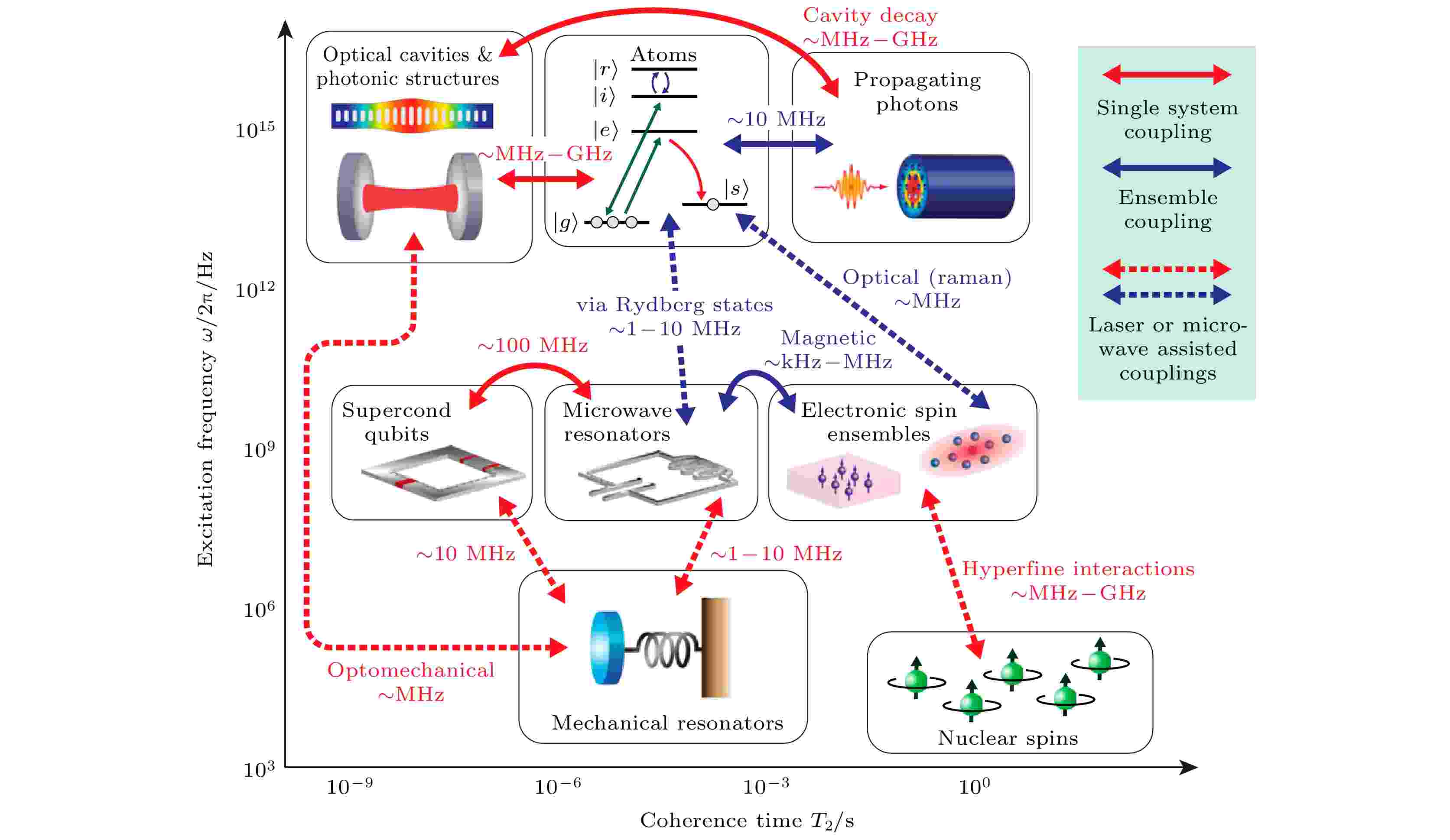
Quantum information is a rapidly emerging field aiming at combining two of the greatest advances in science and technology of the twentieth century, that is, quantum mechanics and information science. To reliably generate, store, process, and transmit quantum information, diverse systems have been studied. While for specific tasks some of these systems are more suitable than others, no single system can meet all envisioned demands. Erbium doped crystal has optical transition at 1.5 μm and possesses long optical coherence time and spin coherence time, and thus is one of the best candidates in building several essential blocks for quantum information applications. In this review, we summarize the applications of erbium doped crystals in quantum memories, quantum transducers, quantum sources, and quantum manipulations based on erbium-erbium interactions. Finally, the outlooks for near term prospects of the mentioned topics are also given.
2022, 71 (6): 066101.
doi:10.7498/aps.71.20212072
Abstract +
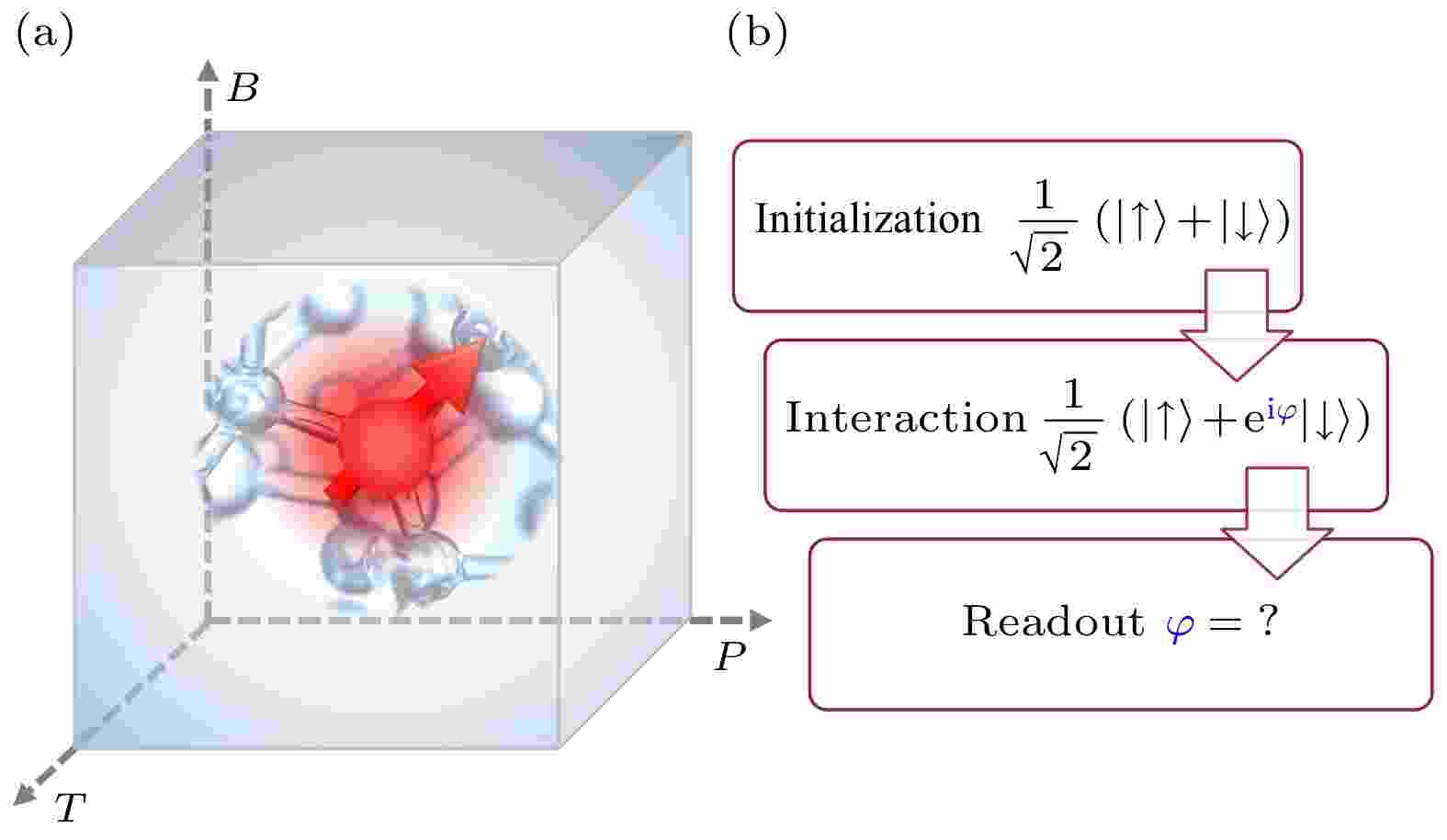
Extreme conditions, such as ultra-low temperatures, high pressures, and strong magnetic fields, are critical to producing and studying exotic states of matter. To measure physical properties under extreme conditions, the advanced sensing schemes are required. As a promising quantum sensor, the diamond nitrogen-vacancy (NV) center can detect magnetic field, electronic field, pressure, and temperature with high sensitivity. Considering its nanoscale spatial resolution and ultra-wide working range, the diamond quantum sensing can play an important role in frontier studies involving extreme conditions. This paper reviews the spin and optical properties of diamond NV center under extreme conditions, including low temperature, high temperature, zero field, strong magnetic fields, and high pressures. The opportunities and challenges of diamond quantum sensing under extreme conditions are discussed. The basic knowledge of spin-based quantum sensing and its applications under extreme conditions are also covered.
2022, 71 (6): 067201.
doi:10.7498/aps.71.20211786
Abstract +
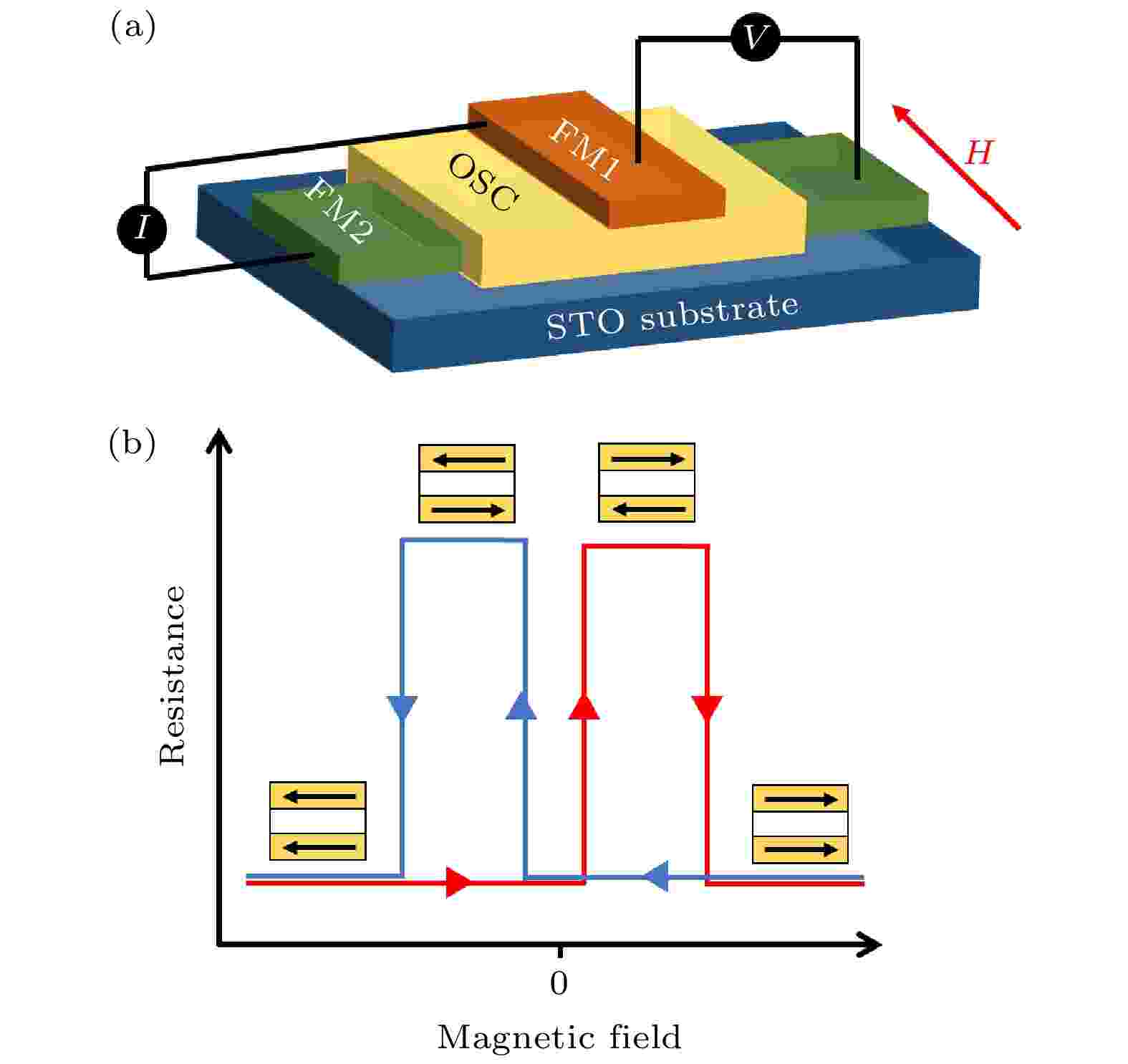
Spintronics are attractive to the utilization in next-generation quantum-computing and memory. Compared with inorganic spintronics, organic spintronics not only controls the spin degree-of-freedom but also possesses advantages such as chemical tailorability, flexibility, and low-cost fabrication process. Besides, the organic spin valve with a sandwich configuration that is composed of two ferromagnetic electrodes and an organic space layer is one of the classical devices in organic spintronics. Greatly enhanced or inversed magnetoresistance (MR) sign appearing in organic spin valve is induced by the unique interfacial effect an organic semiconductor/ferromagnetic interface. The significant enhancement or inversion of MR is later proved to be caused by the spin-dependent hybridization between molecular and ferromagnetic interface,i.e., the spinterface. The hybridization is ascribed to spin-dependent broadening and shifting of molecular orbitals. The spinterface takes place at one molecular layer when attaching to the surface of ferromagnetic metal. It indicates that the MR response can be modulated artificially in a specific device by converting the nature of spinterface. Despite lots of researches aiming at exploring the mechanism of spinterface, several questions need urgently to be resolved. For instance, the spin polarization, which is difficult to identify and observe with the surface sensitive technique and the inversion or enhancement of MR signal, which is also hard to explain accurately. The solid evidence of spinterface existing in real spintronic device also needs to be further testified. Besides, the precise manipulation of the MR sign by changing the nature of spinterface is quite difficult. According to the above background, this review summarizes the advance in spinterface and prospects future controllable utilization of spinterface. In Section 2, we introduce the basic principle of spintronic device and spinterface. The formation of unique spinterface in organic spin valve is clarified by using the difference in energy level alignment between inorganic and organic materials. Enhancement and inversion of MR sign are related to the broadening and shifting of the molecular level. In Section 3, several examples about identification of spinterface are listed, containing characterization by surface sensitive techniques and identification in real working devices. In Section 4 some methods about the manipulation of spinterface are exhibited, including modulation of ferroelectric organic barrier, interface engineering, regulation of electronic phase separation in ferromagnetic electrodes, etc. Finally, in this review some unresolved questions in spintronics are given, such as multi-functional and room-temperature organic spin valve and improvement of the spin injection efficiency. Spinterface is of great importance for both scientific research and future industrial interest in organic spintronics. The present study paves the way for the further development of novel excellent organic spin valves.
2022, 71 (6): 067301.
doi:10.7498/aps.71.20211900
Abstract +
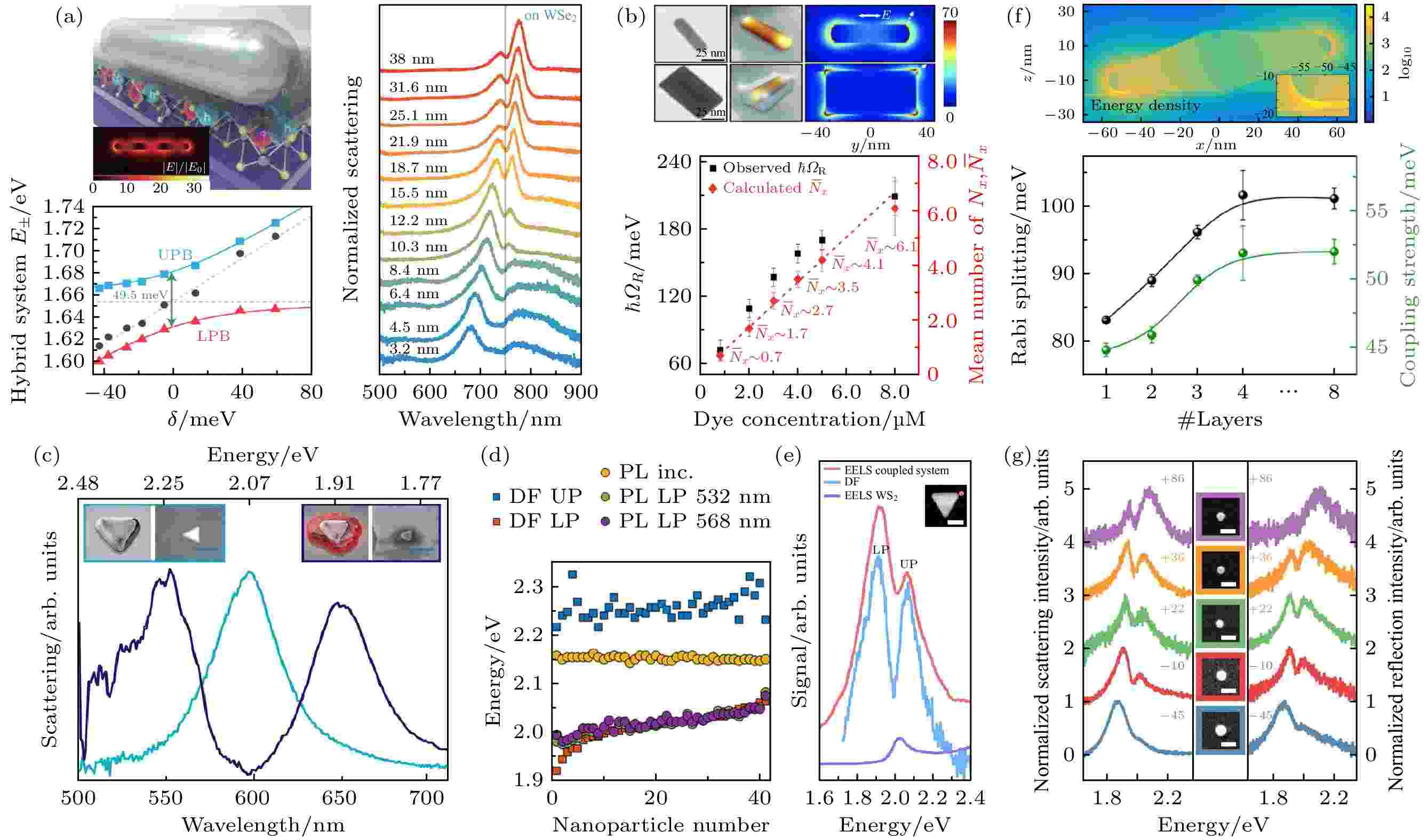
In cavity quantum electrodynamics, when the interaction between quantum emitter and cavity mode is strong enough to overcome the mean decay rate of the system, it will enter into a strong coupling regime, thereby forming part-light part-matter polariton states. Strong coupling can serve as a promising platform for room temperature Bose-Einstein condensation, polariton lasing, single photon nonlinearity, quantum information, etc. Localized surface plasmons supported by single metal nanostructures possess extremely small mode volume, which is favorable for realizing strong coupling. Moreover, the nanoscale dimensions of plasmonic structures can facilitate the miniaturization of strong coupling systems. Here, the research progress of strong plasmon-exciton coupling between single metal nanoparticles/nanogaps and quantum emitters is reviewed. The theory background of strong coupling is first introduced, including quantum treatment, classical coupled oscillator model, as well as the analytical expressions for scattering and photoluminescence spectra. Then, strong coupling between different kinds of plasmonic nanostructures and quantum emitters is reviewed. Single metal nanoparticles, nanoparticle dimers, and nanoparticle-on-mirror structures constitute the most typical plasmonic nanostructures. The nanogaps in the latter two systems can highly concentrate electromagnetic field, providing optical nanocavities with smaller mode volume than single nanoparticles. Therefore, the larger coupling strength can be achieved in the nanogap systems, which is conducive to strong coupling at the single-exciton level. In addition, the active tuning of strong coupling based separately on thermal, electrical and optical means are reviewed. The energy and oscillator strength of the excitons in transition metal dichalcogenide (TMDC) monolayers are dependent on temperature. Therefore, the strong coupling can be tuned by heating or cooling the system. The excitons in TMDC monolayers can also be tuned by electrical gating, enabling electrical control of strong coupling. Optically tuning the quantum emitters provides another way to actively control the strong coupling. Overall, the research on active tuning of strong plasmon-exciton coupling is still very limited, and more investigations are needed. Finally, this review is concluded with a short summary and the prospect of this field.

2022, 71 (6): 067303.
doi:10.7498/aps.71.20211819
Abstract +
The quantum interference effect in single-molecule devices is a phenomenon in which electrons are coherently transported through different frontier molecular orbitals with multiple energy levels, and the interference will occur between different energy levels. This phenomenon results in the increase or decrease of the probability of electron transmission in the electrical transport of the single-molecule device, and it is manifested in the experiment when the conductance value of the single-molecule device increases or decreases. In recent years, the use of quantum interference effects to control the electron transport in single-molecule device has proved to be an effective method, such as single-molecule switches, single-molecule thermoelectric devices, and single-molecule spintronic devices. In this work, we introduce the related theories of quantum interference effects, early experimental observations, and their regulatory role in single-molecule devices.
2022, 71 (6): 067802.
doi:10.7498/aps.71.20212050
Abstract +
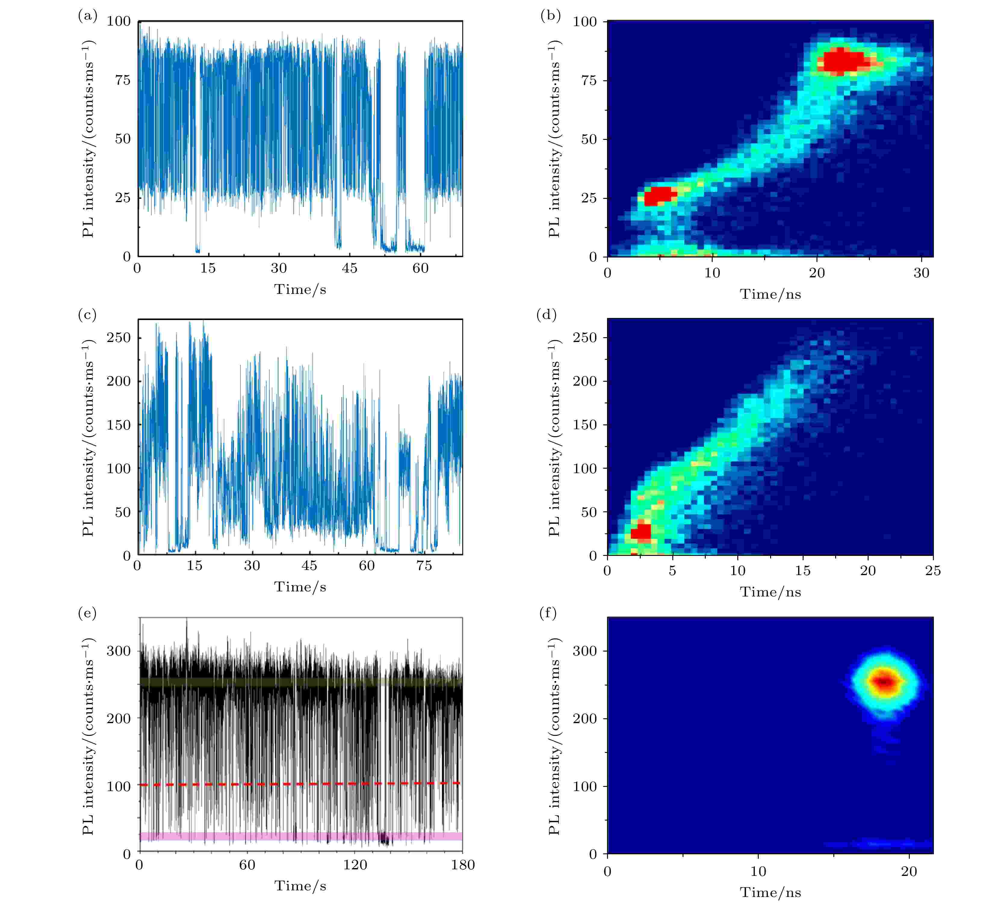
Colloidal semiconductor quantum dots (QDs) have strong light absorption, continuously adjustable narrowband emission, and high photoluminescence quantum yields, thereby making them promising materials for light-emitting diodes, solar cells, detectors, and lasers. Single-QD photoluminescence spectroscopy can remove the ensemble average to reveal the structure information and exciton dynamics of QD materials at a single-particle level. The study of single-QD spectroscopy can provide guidelines for rationally designing the QDs and giving the mechanism basis for QD-based applications. We can also carry out the research of the interaction between light and single QDs on a nanoscale, and prepare QD-based single-photon sources and entangled photon sources. Here, we review the recent research progress of single-QD photoluminescence spectroscopy and exciton dynamics, mainly including photoluminescence blinking dynamics, and exciton and multi-exciton dynamics of single colloidal CdSe-based QDs and perovskite QDs. Finally, we briefly discuss the possible future development trends of single-QD spectroscopy and exciton dynamics.

2022, 71 (6): 068502.
doi:10.7498/aps.71.20211872
Abstract +
Magnetic field effects (MFEs) are used to describe the changes of the photophysical properties (including photoluminescence, electroluminescence, injectedcurrent, photocurrent, etc.) when materials and devices are subjected to the external magnetic field. The MFEs in non-magnetic luminescent materials and devices were first observed in organic semiconductor. In the past two decades, the effects have been studied extensively as an emerging physical phenomenon, and also used as a unique experimental method to explore the processes such as charge transport, carrier recombination, and spin polarization in organic semiconductors. Recent studies have found that the MFEs can also be observed in metal halide perovskites with strong spin-orbital coupling. Besides, for expanding the research domain of MFEs, these findings can also be utilized to study the physical mechanism in metal halide perovskites, and then provide an insight into the improving of the performance of perovskite devices. In this review, we focus on the magnetic field effects on the electroluminescence and photoluminescence changes of organic semiconductors and halide perovskites. We review the mainstream of theoretical models and representative experimental phenomena which have been found to date, and comparatively analyze the luminescence behaviors of organic semiconductors and halide perovskites under magnetic fields. It is expected that this review can provide some ideas for the research on the MFEs of organic semiconductors and halideperovskites, and contribute to the research of luminescence in organic materials and halideperovskites.
2022, 71 (6): 060303.
doi:10.7498/aps.71.20211797
Abstract +
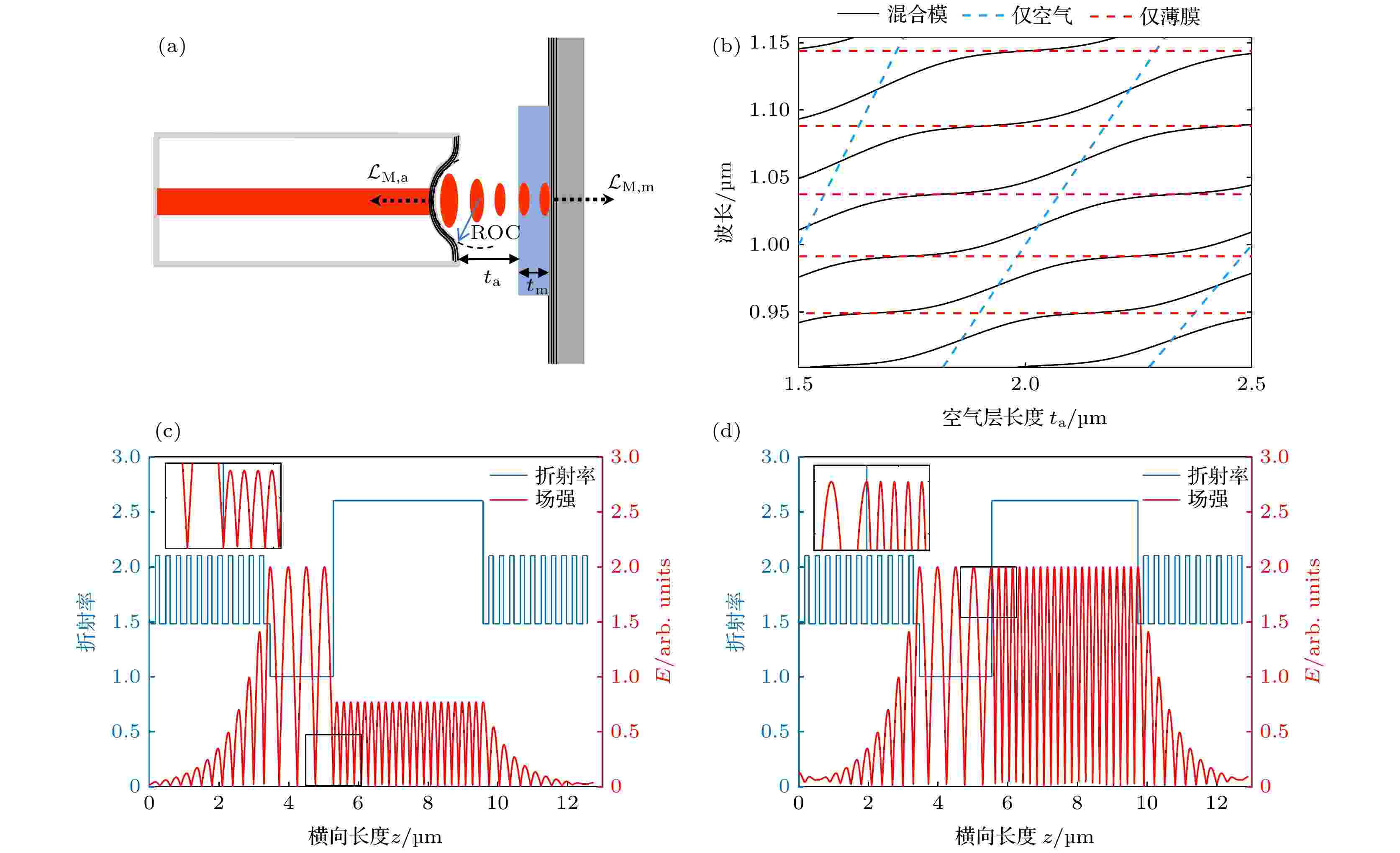
Single spin color centers in solid materials are one of the promising candidates for quantum information processing, and attract a great deal of interest. Nowadays, single spin color centers in silicon carbide, such as divacancies and silicon vacancies have been developed rapidly, because they not only have similar properties of the NV centers in diamond, but also possess infrared fluorescence that is more favorable for transmission in optical fiber. However, these centers possess week fluorescence with broad spectrum, which prevents some key technologies from being put into practical application, such as quantum key distribution, photon-spin entanglement, spin-spin entanglement and quantum sensing. Therefore, optical resonator is very suitable for coupling centers to filter their spectrum and enhance the fluorescence by Purcell effect. It is very advantageous to use the fiber end face as cavity mirrors, thereby the fiber can provide small cavity volume corresponding to a large enhancement in spin color centers, and collect the fluorescence in cavity simultaneously, which has no extra loss in comparison with other collection methods. In this work, the properties and performance of fiber Fabry-Perot cavity coupling silicon carbide membrane are mainly studied through theoretical calculation. Firstly, some parameters are optimized such as membrane roughness and mirror reflection by calculating the mode of the fiber cavity and enhancing the color centers coupling into the cavity, then analyzing the properties of different modes in cavity, the enhancement effect on cavity coupling color centers, and other relevant factors affecting the cavity coupling color centers. Next, the influences of dominated factor and vibration on the properties of the cavity, the enhancement and outcoupling of centers coupled into the cavity are investigated, and finally the optimal outcoupling efficiency corresponding to different vibration intensities is obtained. These results give direct guidance for the further experimental design and direction for optimization of the fiber cavity coupling color centers.
2022, 71 (6): 063301.
doi:10.7498/aps.71.20212003
Abstract +
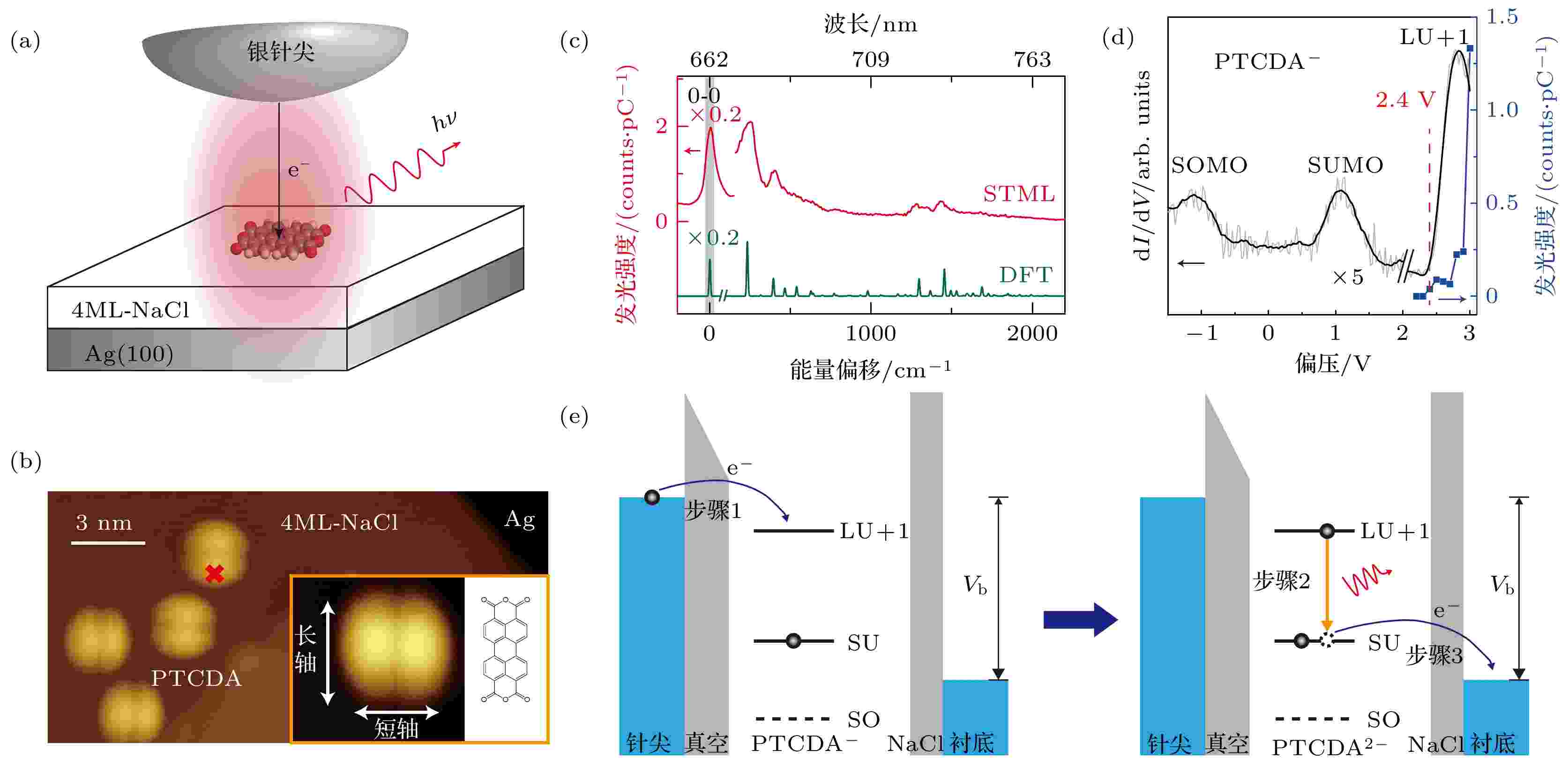
The intramolecular vibronic coupling has a great effect on molecular electronic transitions and associated spectral characteristics, which is a central topic in the study of molecular spectroscopy. In this paper, we investigate the vibronic coupling of a transiently charged state within a single 3,4,9,10-perylenetetracarboxylicdianhydride (PTCDA) molecule in real space by imaging the spatial distribution of single-molecule electroluminescence via highly localized excitation of tunneling electrons in a plasmonic nanocavity. The electron injections from a scanning tunneling microscope tip into a PTCDA molecule on a silver-supported ultrathin salt layer produce a transient doubly charged molecular anion that emits vibrationally resolved fluorescence. The sub-molecular resolved spectroscopic imaging for the –2 valence transiently charged state shows a two-spot pattern along the molecular short axis for the purely electronic 0-0 transition. However, the observed two-spot orientation for certain anti-symmetric vibronic-state imaging is found to be evidently different from the purely electronic 0-0 transition, rotating 90°, which reflects the change in the transition dipole orientation from along the molecular short axis to the long axis. Such a change directly reveals the occurrence of strong vibronic coupling associated with a large Herzberg-Teller (HT) contribution, which goes beyond the conventional Franck-Condon (FC) picture. Combined with theoretical calculations, the anti-symmetric vibration is found to have a strong dynamic disturbance to the transition density of purely electronic transitions, especially those atoms with large transition densities, which induces a strong transition charge oscillation along the long axis of the molecule and thus leads to a transition dipole along the long axis of the molecule. On the other hand, for vibronic emissions associated with the totally symmetric molecular vibration (such as the v1(Ag) mode described above), the observed two-spot orientation in the vibronic-state imaging pattern is found to be the same as the purely electronic 0-0 transition, which directly reveals its FC-dominated nature. Notably, the vibration-induced emission associated with HT-dominated contributions (such as the v2(B3g) mode) is often discussed in the literature by using an intensity borrowing mechanism via the state mixing with other high-lying eigenstates. In the present work, the v2-vibration with B3gsymmetry is likely to modulate the zero-order electronic wavefunction of the S1state in a way to best resemble that of the S2state (i.e., induce efficient mixing of the electronic excited state S1with the electronic excited state S2), so that the v2-vibration induced emission seems to borrow intensities from neighboring S2→S0transitions. Our results provide a new route for the real-space understanding of the microscopic picture for the vibronic coupling within a single molecule in a transiently charged state.
2022, 71 (6): 067202.
doi:10.7498/aps.71.20211815
Abstract +
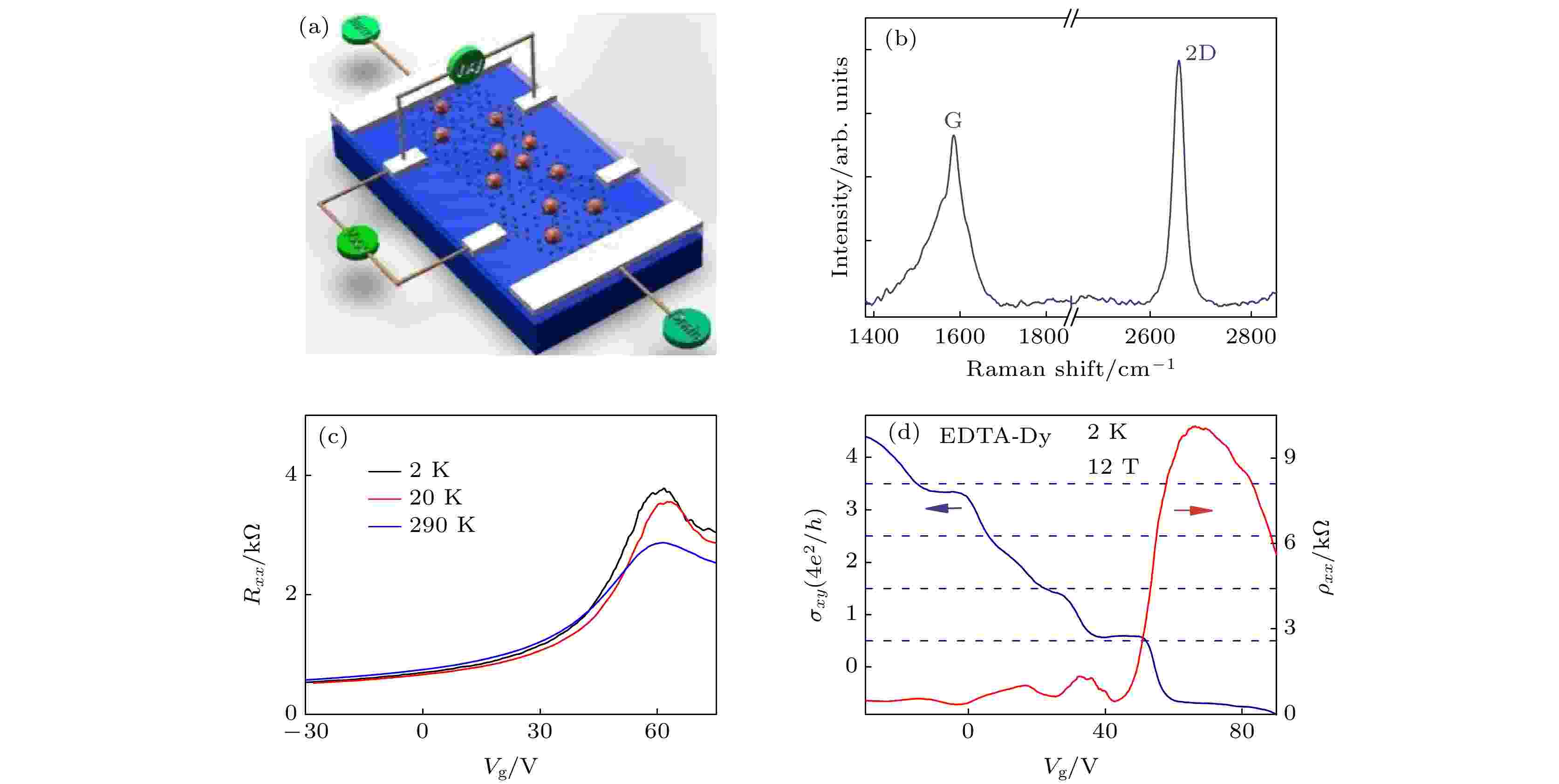
In order to enhance the spin orbit interaction (SOI) in graphene for seeking the dissipationless quantum spin Hall devices, unique Kane-Mele-type SOI and high mobility samples are desired. However, the common external modification of graphene often introduces “extrinsic” Rashba-type SOI, which will destroy the possible topological state, bring a certain degree of impurity scattering and reduce the sample mobility. Here we show that by the EDTA-Dy molecule dressing, the carrier mobility is even improved, and the quantum Hall plateaus are observed more clearly. The Kane-Mele type SOI is mimicked after dressing, which is evidenced by the suppressed weak localization at equal carrier densities and simultaneous Elliot-Yafet spin relaxation. This is attributed to the spin-flexural phonon coupling induced by the enhanced graphene ripples, as revealed by the in-plane magnetotransport measurement.
COVER ARTICLE
2022, 71 (6): 067601.
doi:10.7498/aps.71.20211348
Abstract +
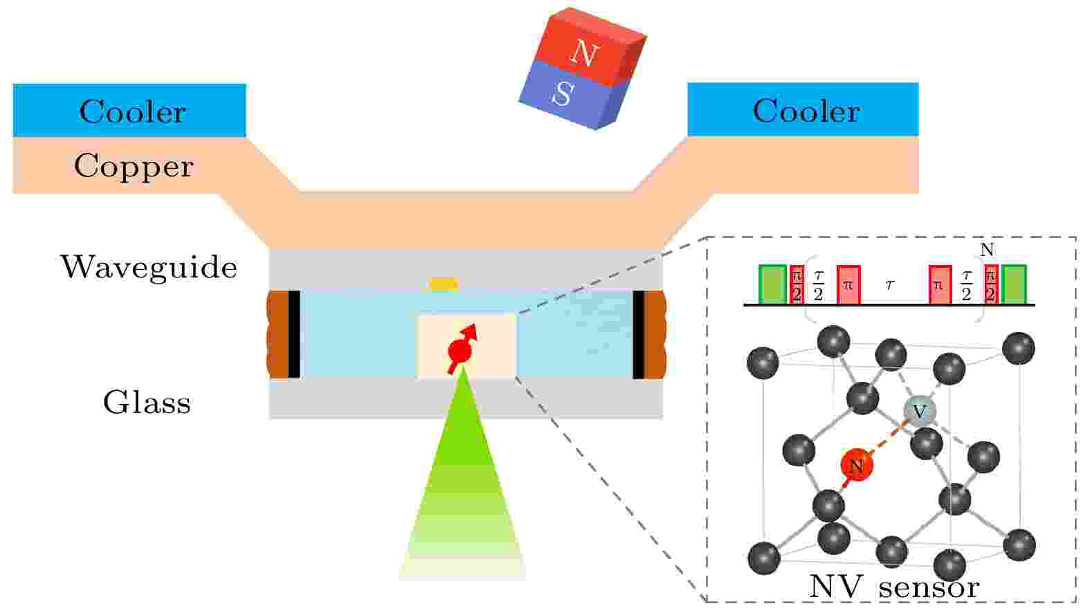
Water is one of the most important substances in the world. It is a crucial issue to study the dynamics of water molecules at interfaces or in the confined systems. In recent years, the emerging magnetic resonance technique based on nitrogen-vacancy (NV) center has allowed us to observe the nanoscale nuclear magnetic signal and temperature simultaneously. Here we succeed in measuring the nuclear magnetic resonance (NMR) signals of nanoscale solid and liquid water on diamond surface by NV center, and observing the solid-liquid phase transition of these nano-water by temperature control. This work demonstrates that the nano-NMR technique based on NV centers can probe the dynamics behavior of nanoscale materials effectively, providing a new way for studying the nanoscale confined systems.
2022, 71 (6): 067801.
doi:10.7498/aps.71.20211858
Abstract +
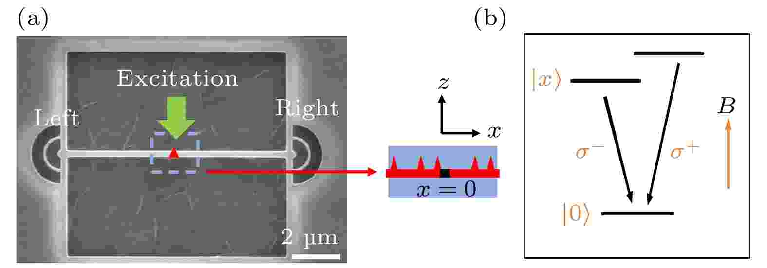
In order to realize scalable and integrated quantum photonic networks, various functional devices are highly desired. Strip waveguides with unidirectional transmission function have a wide range of applications in devices such as single-photon diodes, transistors and deterministic quantum gate devices. In this work, the separation of circularly polarized light is achieved by exciting a quantum dot light source in a central region of a waveguide at a low temperature of 4.2 K by using a confocal microscope system. By applying a magnetic field with Faraday configuration (along with the quantum dot growth direction), the spin-momentum locking effect in the waveguide is verified. Both forward shift and reverse shift of different values of output photon energy are demonstrated to show the unidirectional transmission of the waveguide. The chiral transmission of quantum dot with anomalous diamagnetic behavior is achieved in experiment, leading to a wider range of wavelength tuning for chrial transmission in a single waveguide. This paper provides a basis for investigating the chiral quantum devices in a wide wavelength range and expands the applications of waveguides in the field of optical quantum information.
2022, 71 (6): 067804.
doi:10.7498/aps.71.20211863
Abstract +
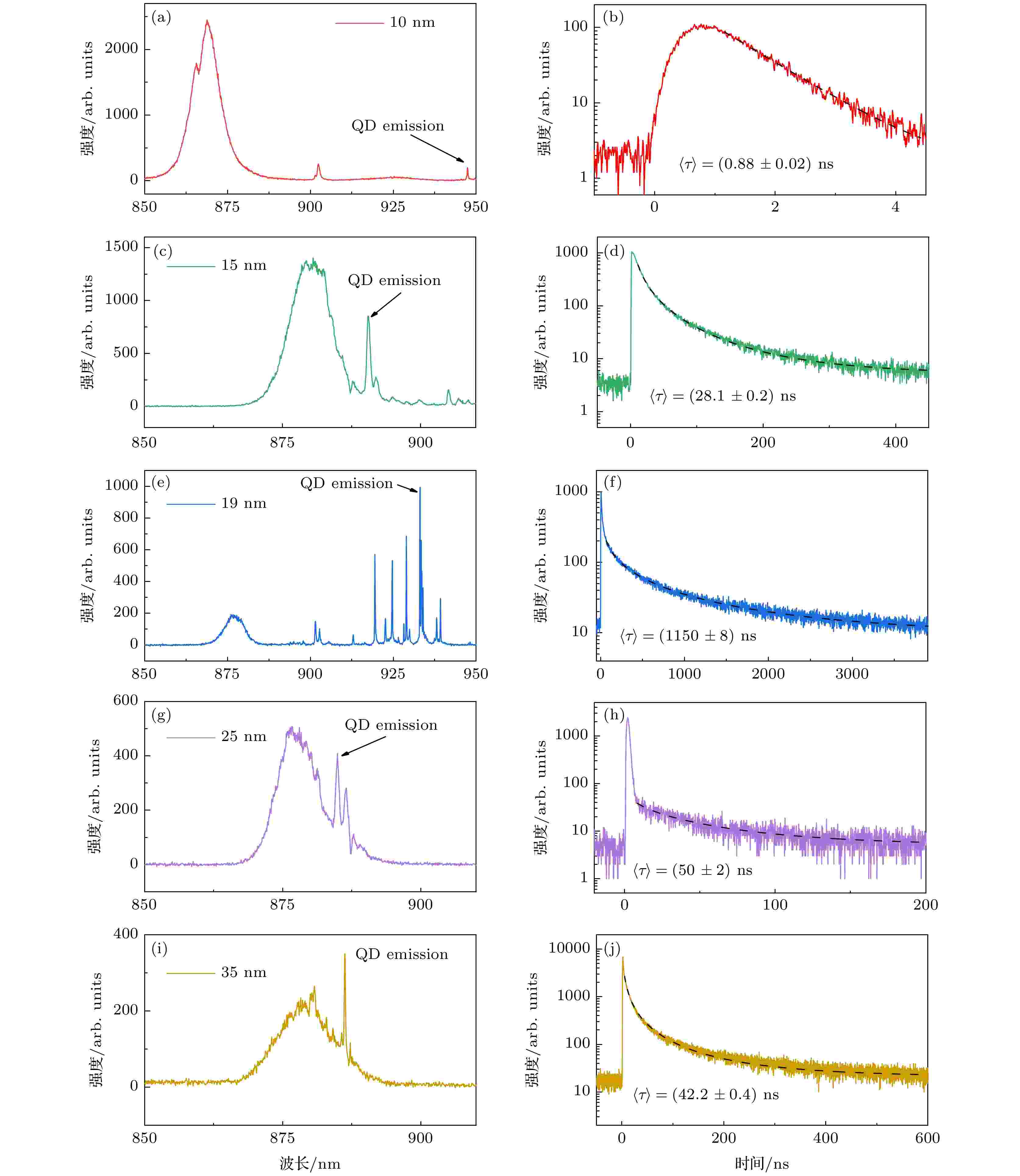
As an ideal single-photon source, quantum dots (QDs) can play a unique role in the field of quantum information. Controlling QD exciton spontaneous emission can be achieved by anti-phase coupling between QD exciton dipole field and Au dipole field after QD film has been transferred onto the Si substrate covered by Au nanoparticles. In experiment, the studied InAs/GaAs QDs are grown by molecular beam epitaxy (MBE) on a (001) semi-insulation substrate. The films containing QDs with different GaAs thickness values are separated from the GaAs substrate by etching away the AlAs sacrificial layer and transferring the QD film to the silicon wafer covered by Au nanoparticles with a diameter of 50 nm. The distanceD(thickness of GaAs) from the surface of the Au nanoparticles to the QD layer is 10, 15, 19, 25, and 35 nm, separately. A 640-nm pulsed semiconductor laser with a 40-ps pulse length is used to excite the QD samples for measuring QD exciton photoluminescence and time-resolved photoluminescence spectra at 5 K. It is found that when the distanceDis 15–35 nm the spontaneous emission rate of exciton is suppressed. And whenDis close to 19 nm, the QD spontaneous emission rate decreases to
$ ~{10}^{-3} $
, which is consistent with the theoretical calculations. The physical mechanism of long-lived exciton luminescence observed in experiment lies in the fact that Au nanoparticles scatter the light field of the exciton radiation in the QD wetting layer, and the phase of the scattered field is opposite to the phase of the exciton radiation field. Therefore, the destructive interference between the exciton radiation field and scattering field of Au nanoparticles results in long-lived exciton emission observed in experiment.
REVIEW
EDITOR'S SUGGESTION
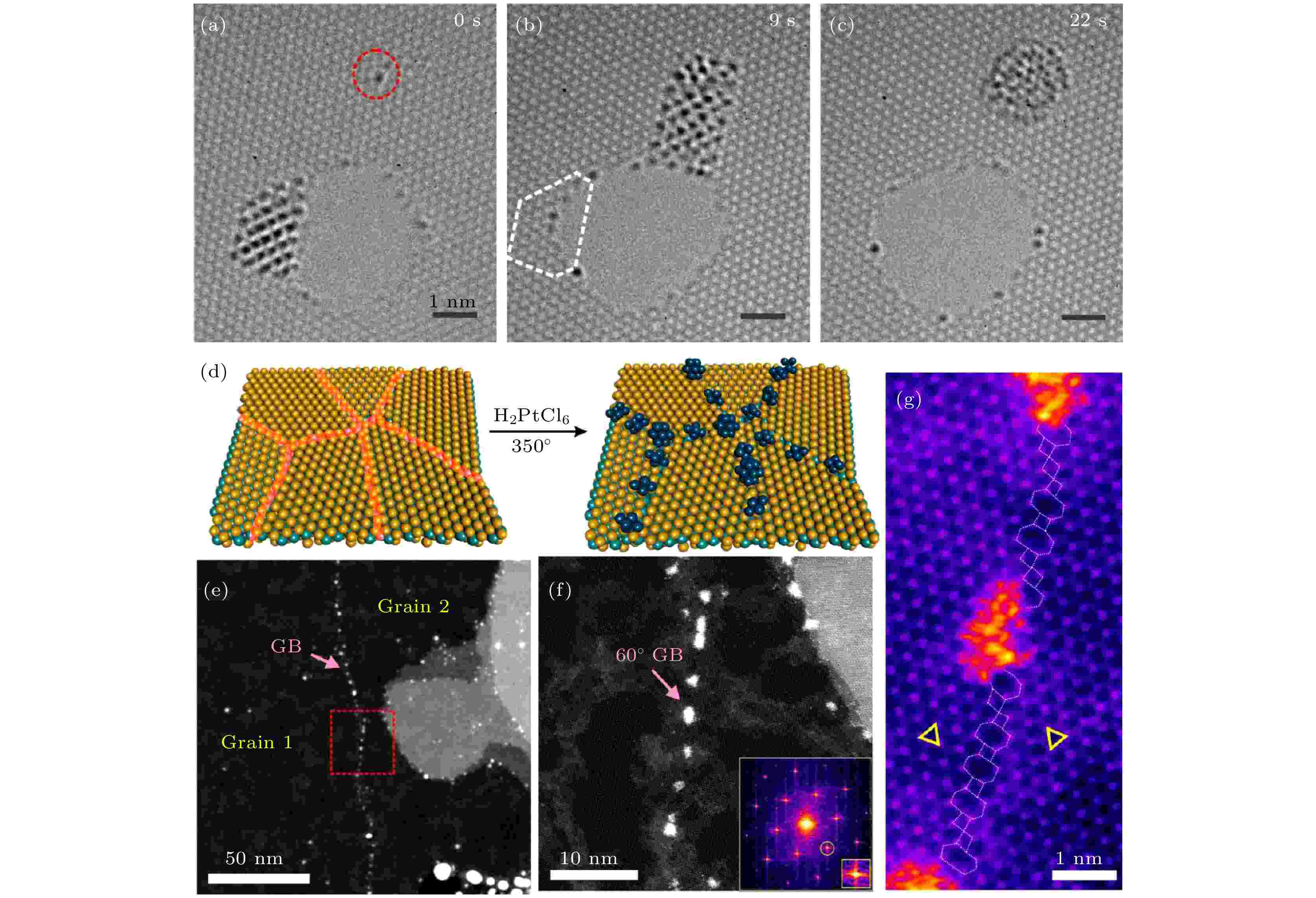
2022, 71 (6): 066801.
doi:10.7498/aps.71.20211902
Abstract +
EDITOR'S SUGGESTION
2022, 71 (6): 068701.
doi:10.7498/aps.71.20211850
Abstract +
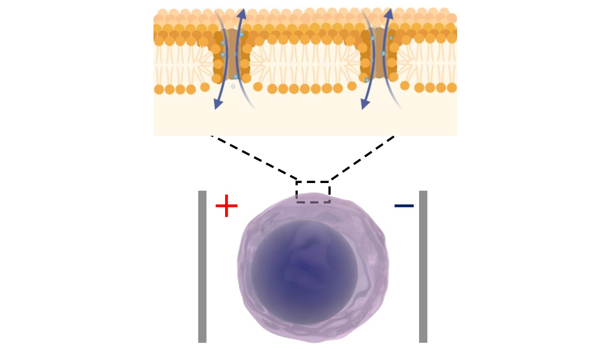
The biomedical application of high-voltage nanosecond pulsed electric fields (nsPEFs) has become an emerging interdisciplinary research field in recent years. Compared with microsecond and millisecond pulsed electric fields, high-voltage nsPEFs can not only lead the cell membrane structure to polarize and dielectric break down the cell membrane structure, i.e. membrane electroporation, but also penetrate into the cell, triggering off organelle bioelectrical effects such as cytoskeleton depolymerization, intracellular calcium ion release, and mitochondrial membrane potential dissipation. Extensive attention has been attracted from related academic communities. In this article, the following aspects are involved. First, the physical model of high-voltage nsPEFs and its bioelectrical effects on cellular organelles are introduced. Then, the existing researches of the interactions of high-voltage nsPEFs with cytoskeleton, mitochondria, endoplasmic reticulum, cell nucleus and other subcellular structure are reviewed and summarized; the relationship between the influence on cellular organelles by high-voltage nsPEFs and the biological effects such as cell death and intercellular communication is highlighted. Finally, the key technical challenges to high-voltage nsPEFs in biomedical research are condensed, followed by the prospects of future research directions.
NUCLEAR PHYSICS

2022, 71 (6): 062301.
doi:10.7498/aps.71.20211839
Abstract +
The effective liquid drop model (ELDM) and the generalized liquid drop model (GLDM) are extended to the case of studying the two-proton (2p) radioactivity from the excited states of proton-rich nuclei. It is shown that the experimental 2p decay half-lives are reproduced well by the ELDM and the GLDM. Then, the 2p decay half-lives of excited states of some nuclei that are not yet available experimentally are predicted by the two models, which are useful for searching for the new 2p decay candidates in future. Meanwhile, the above predicted half-lives are analyzed and compared with those given by the unified fission model (UFM). Next, the influence of the uncertainties of the decay energy and the angular momentum on the half-lives are analyzed in the frame of the two models by taking the 2p radioactivity of the 21+isomeric state of94Ag for example. It is found that the half-lives go up with the increase of the angular momentum, following the law of the quadratic function. Furthermore, the strong dependence of the half-lives on the decay energy suggests that it is important and necessary to measure accurately the mass value of the parent nucleus and the daughter nucleus and the excitation energy. Finally, it is necessary to point out that the existence of the 2p radioactivity in the 21+isomeric state of94Ag remains to be a mystery. Moreover, although the 2p radioactivity is observed from the higher excited states of17Ne and18Ne, the relevant hypotheses have not yet been further tested experimentally. The construction of a new generation of radioactive ion beam facilities, such as the high intensity heavy-ion accelerator facility (HIAF), is expected to be used to uncover the nature of the 2p radioactivity in the 21+isomeric state of94Ag and further test the hypotheses of the 2p decay from the higher excited states of17Ne and18Ne. On the other hand, some microscopic models, such as the shell model, need to be further developed by including some necessary physical factors, such as the tensor force, three-body force and accurate pairing force, to describe the mechanism of the 2p emission of the excited states more reasonably. In summary, more nuclear structure information can be extracted by studying the 2p radioactivity of the excited states. It is worth studying further although it is rather difficult to observe.
ELECTROMAGNETISM, OPTICS, ACOUSTICS, HEAT TRANSFER, CLASSICAL MECHANICS, AND FLUID DYNAMICS
2022, 71 (6): 064101.
doi:10.7498/aps.71.20211204
Abstract +
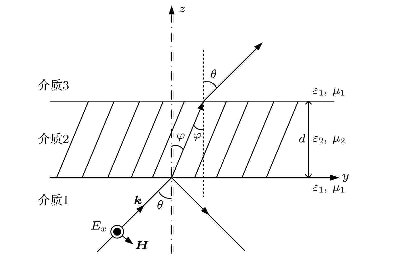
Based on the generalized Zakharov model, a numerical model of electromagnetic wave propagating in the ionosphere at different angles is established by combining the finite difference time domain (FDTD) method of obliquely incident plasma with the double hydrodynamics equation and through equivalently transforming the two-dimensional Maxwell equation into one-dimensional Maxwell equation and the plasma hydrodynamics equation. In this paper. the dominant equation of Z-wave in obliquely incident nonlinear ionospheric plasma having been analyzed and deduced, the FDTD algorithm suitable for calculating the propagation characteristics of ionospheric electromagnetic wave is deduced. The simulation results prove the accuracy and effectiveness of this method for the Langmuir disturbance caused by electromagnetic wave heating the ionosphere at a small inclination angle. The results show that under small angle incidence, the high-power high-frequency electromagnetic wave excites the Langmuir wave near the O-wave reflection point in the ionospheric plasma. At the same time, the wave particle interaction causes the O-wave to convert into Z-wave and propagate into the higher region of the ionosphere. In this work, the electromagnetic wave propagation characteristics are further studied based on ionospheric plasma, which is helpful in laying the foundation of numerical algorithm for comprehensively and in depth analyzing the influence of ionospheric Langmuir disturbance on ionospheric radio wave propagation characteristics.
EDITOR'S SUGGESTION
2022, 71 (6): 064201.
doi:10.7498/aps.71.20211582
Abstract +
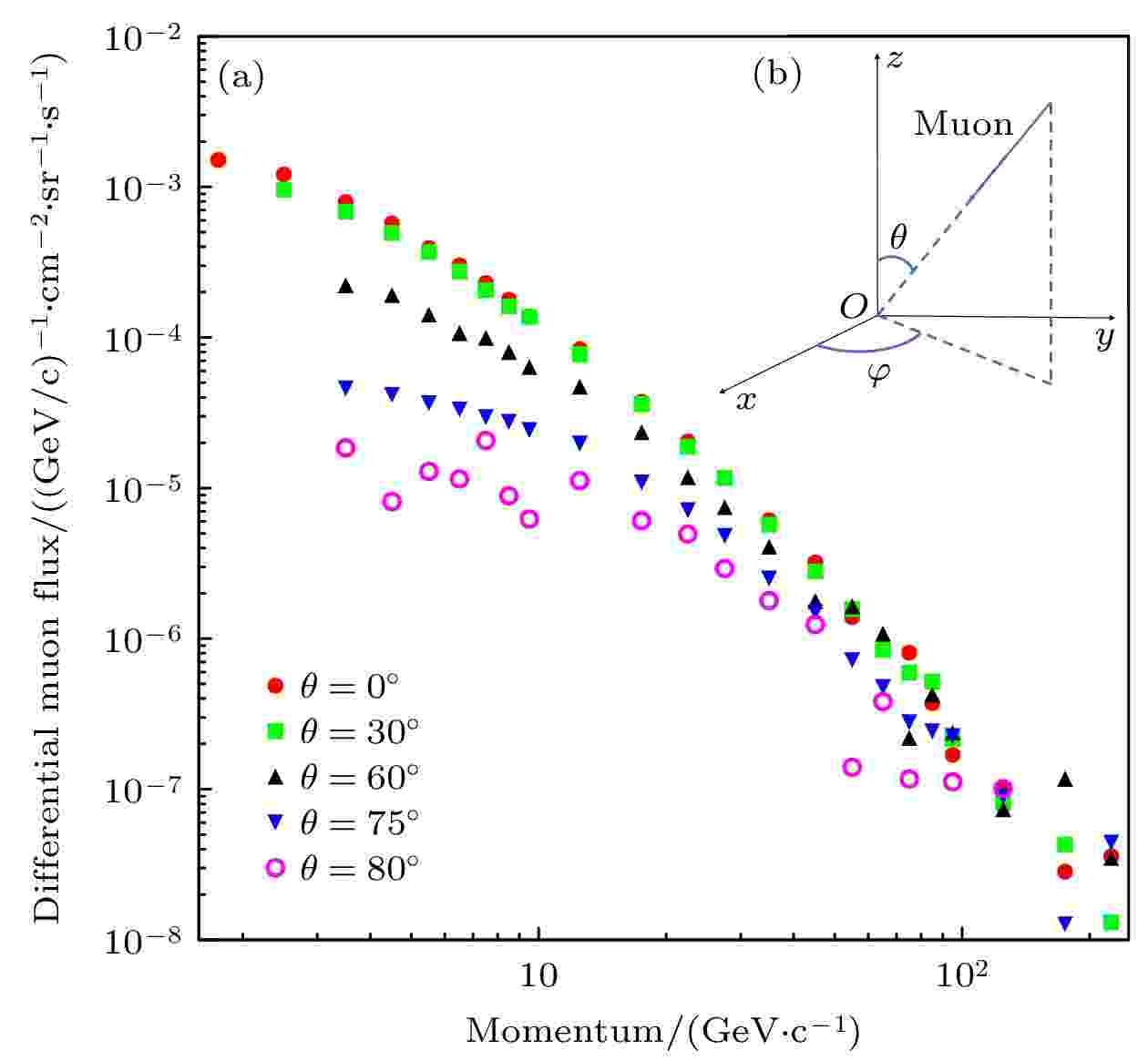
Muon radiography is a nondestructive imaging technology based on the naturally existing cosmic ray muons. Because cosmic ray muons have the strong ability to penetrate, muon radiography in which the absorption of muons through matter is utilized, is especially suitable for the imaging of large-scale objects. While the traditional geophysical technologies used in archeology have some limitations, muon radiography is expected to become a powerful supplement in the nondestructive detection of large-scale cultural relics. Based on Monte Carlo simulation method Geant4, the muon radiography of the underground palace of Qinshihuang Mausoleum is studied in this work. A model of the underground palace of Qinshihuang Mausoleum is set up with GEANT4 program according to the data acquired by the previous archaeological study of Qinshihuang Mausoleum’s inner structure, as well as a reference model without these inner structure. By investigating the differences between the muon fluxes obtained from the two models, the muon radiography image of the inner structure of the model can be obtained. During the simulation, the cosmic ray muon source is generated by sampling according to an empirical formula summarized by Reyna, which can accurately describe the energy spectrum and angular distribution of cosmic ray muons at sea level. In addition, two viewpoints are selected in order to determine the three-dimensional position of the chamber. The simulation data are processed by using an image reconstruction algorithm which can be described as the following three steps. Firstly, the counts of muons in different directions are converted into muon flux. Secondly, the muon flux of the reference model is deducted from that of the Qinshihuang Mausoleum model, and the angular coordinates of the chamber walls are determined. Finally, combined with the wall’s angular coordinates obtained from the two viewpoints and the relative position between the two viewpoints, the chamber size and its position are reconstructed according to the geometric relationship. The errors of the reconstructed chamber center position and the length of chamber walls are both approximately 7%. In this article, we conduct only a preliminary study of muon radiography applied to the nondestructive detection of Qinshihuang Mausoleum, but the results show that muon radiography can be a promising tool for the archeological study of Qinshihuang Mausoleum. In the follow-up study, more factors will be taken into consideration, including the details of Qinshihuang Mausoleum model, and the improvement of image reconstruction algorithm.
2022, 71 (6): 064202.
doi:10.7498/aps.71.20211758
Abstract +

EDITOR'S SUGGESTION
2022, 71 (6): 064204.
doi:10.7498/aps.71.20212132
Abstract +
We report on a 1550-nm vertical-cavity surface-emitting laser (VCSEL) with single mode power of 0.97 mW. The quaternary AlGaInAs quantum well is designed to improve the gain level in an active region. The mesa structure with tunneling capability is designed and fabricated to achieve the efficient carrier injection and the transverse mode guiding. The distributed Bragg reflector (DBR) mirror of 1550 nm VCSEL consists of the semiconductor DBR and outer dielectric DBR. The central wavelength of VCSEL is 1547.6 nm. The maximum output power of 2.6 mW is achieved at 15 ℃, and the maximum single-mode output power is 0.97 mW. The side mode suppression ratio (SMSR) can reach more than 35 dB. The maximum output power decreases with operation temperature increasing. However, the maximum output power of more than 1.3 mW is also gained at 35 ℃. The shift coefficient of the central wavelength varying with the operation current is 0.13 nm/mA. And the wavelength shows a stable shift with the operation current in the single-mode working region, which indicates the application possibility in the field of gas detection.
2022, 71 (6): 064205.
doi:10.7498/aps.71.20211882
Abstract +
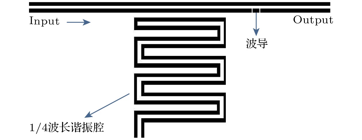
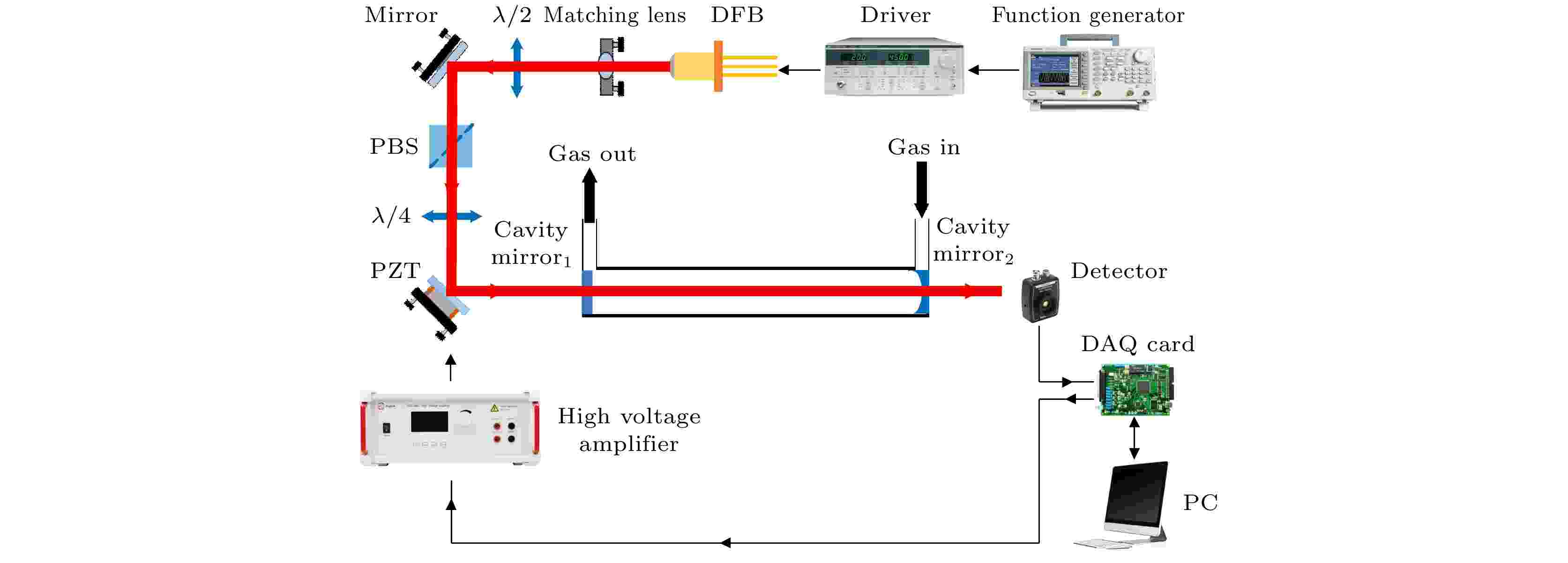
In this paper, an efficient method of suppressing interference is presented in an optical feedback-cavity enhanced absorption spectroscopy (OF-CEAS) system. The Ariy function is used to analyze the interference signal in the transmission cavity mode signal. It is found that the interference signal in system originates from multiple reflections of the beam in the mirror, which is verified by replacing three kinds of cavity front mirrors with different thickness values. The result obtained by the Ariy function is used as a background signal, and the absorption spectrum signal can be obtained by making its difference from the absorption signal of the measured gas. This method effectively avoids the frequency error caused by the inability to measure the background signal and the absorption signal at the same time in the OF-CEAS system. Finally, the absorption characteristics of acetylene gas at 1.53 μm are measured. Based on the signal-to-noise ratio, the detection sensitivity of the system is evaluated to be 7.143 × 10⁻⁸(1σ). Experiments show that this method is effective in improving the detection sensitivity of OF-CEAS system.
2022, 71 (6): 064701.
doi:10.7498/aps.71.20211682
Abstract +
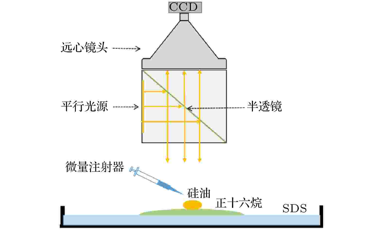
Surface tension gradient due to concentration difference and temperature difference induces liquid convection, known as Marangoni effect. The Marangoni effect has been extensively studied to understand its fundamental physics and its industrial applications. In this paper we study Marangoni effect of droplet in a three-phase liquid system. In this system, silicone oil is chosen as a driving liquid, and n-hexadecane is used as a driven liquid. A high-speed camera is used to capture the spreading process of n-hexadecane driven by silicon oil on the sodium dodecyl sulfate (SDS) solution. The experiment shows that n-hexadecane driven by silicone oil spreads from inside out, forming a ring structure. According to spreading dynamic behavior of internal boundary and external boundary of n-hexadecane ring, we study the spreading pattern of internal boundary and external boundary of n-hexadecane ring, and the influence of silicone oil volume on the spreading process. Analysis shows that the spreading law of internal silicone oil conforms to single droplet spreading at the liquid interface. In the initial spreading stage, the spreading of four-phase contact line (internal boundary) among silicone oil, air, n-hexadecane and water are dominated by gravity, The scale law of spreading distanceRof four-phase contact line andtis in a range of
$ R \sim {t}^{1/4} $
-
$ R \sim {t}^{1/2} $
. Owing to the gravity influence, the larger the volume of silicone oil, the faster the four-phase contact line spreads. The volume of silicone oil has no effect on the scaling law of the whole spreading process. The next spreading stage, the spreading of the contact line is dominated by the interfacial tension gradient. The scale law of spreading distanceRandtconforms to
$ R \sim {t}^{3/4} $
. Under silicone oil driven, the liquid thickness of n-hexadecane at the four-phase contact line (internal boundary) among air, silicone oil, N-hexadecane and water increases, thus changing the contact angle at three-phase contact line (external boundary) among air, n-hexadecane and water. The change of contact angle leads the interfacial tension gradient to produce. The interfacial tension gradient drives external boundary to spread. Because the spreading of the three-phase contact line is dominated by interfacial tension gradient, the scale law of spreading distanceRof three-phase contact line and timetconforms to
$ \sim {t}^{3/4} $
.
CONDENSED MATTER: STRUCTURAL, MECHANICAL, AND THERMAL PROPERTIES

2022, 71 (6): 066401.
doi:10.7498/aps.71.20211757
Abstract +
Based on an effective single cluster growth algorithm, bond percolation on square lattice with the nearest neighbors, the next nearest neighbors, up to the 5th nearest neighbors are investigated by Monte Carlo simulations. The bond percolation thresholds for more than 20 lattices are deduced, and the correlations between percolation threshold
$p_{\rm c}$
and lattice structures are discussed in depth. By introducing the index
$\xi = \displaystyle\sum\nolimits_{i} z_{i} r_{i}^{2} / i$
to remove the degeneracy, it is found that the thresholds follow a power law
$p_{\rm c} \propto \xi^{-\gamma}$
, with
$\gamma \approx 1$
, where
$z_{i}$
is theith neighborhood coordination number, and
$r_{i}$
is the distance between sites in thei-th coordination zone and the central site.
EDITOR'S SUGGESTION
2022, 71 (6): 066402.
doi:10.7498/aps.71.20211714
Abstract +
Antimony selenide (Sb2Se3) is a promising low-cost and environmentally-friendly semiconductor photovoltaic material. The power conversion efficiency of Sb2Se3solar cells has been improved to
$ \sim $
10% in the past few years. The carrier recombination transfer dynamics is significant factor that affects the efficiency of Sb2Se3solar cells. In this work, carrier recombination on the Sb2Se3surface and carrier transfer dynamics at the CdS/Sb2Se3heterojunction interface are systematically investigated by surface transient reflectance. According to the evolution of relative reflectance change
${{\Delta }{R}}/{{R}}$
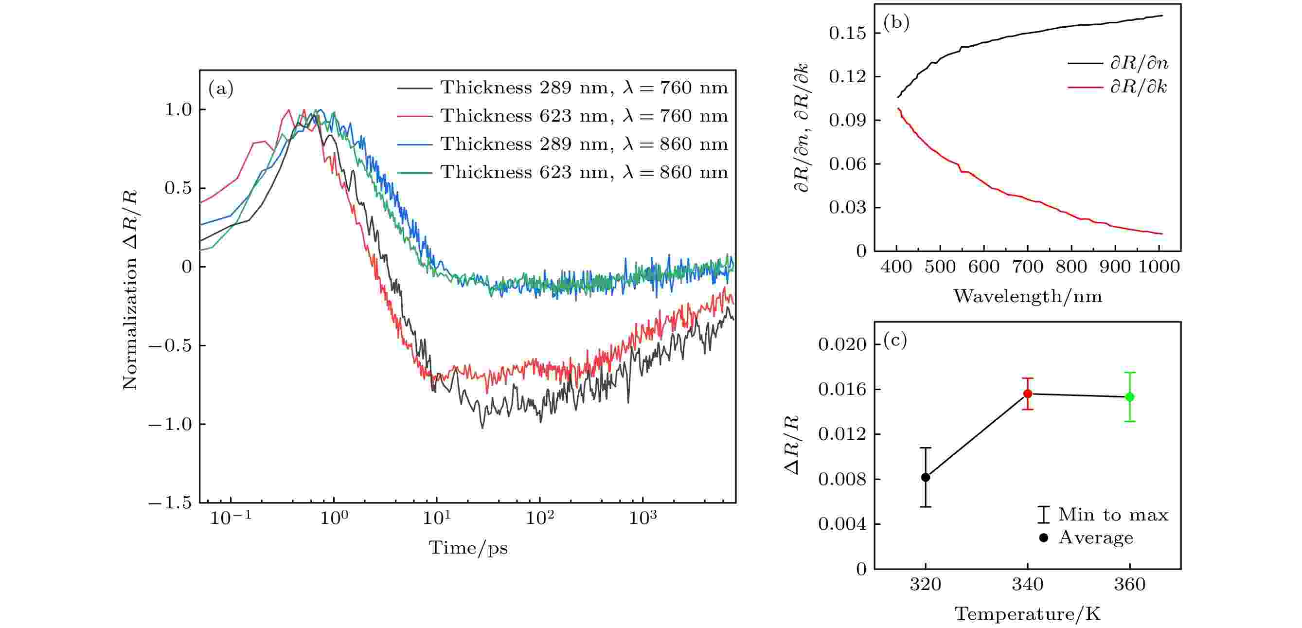
, the carrier thermalization and band gap renormalization time of Sb2Se3are determined to be in a range from 0.2 to 0.5 ps, and carrier cooling time is estimated to be about 3-4 ps. Our results also demonstrate that both free electron and shallow-trapped electron transfer occur at the Sb2Se3/CdS interface after photo excitation. Our results present a method of explaining the transient reflectance of Sb2Se3and enhancing the understanding of carrier kinetics at Sb2Se3surface and Sb2Se3/CdS interface.
2022, 71 (6): 066501.
doi:10.7498/aps.71.20211405
Abstract +
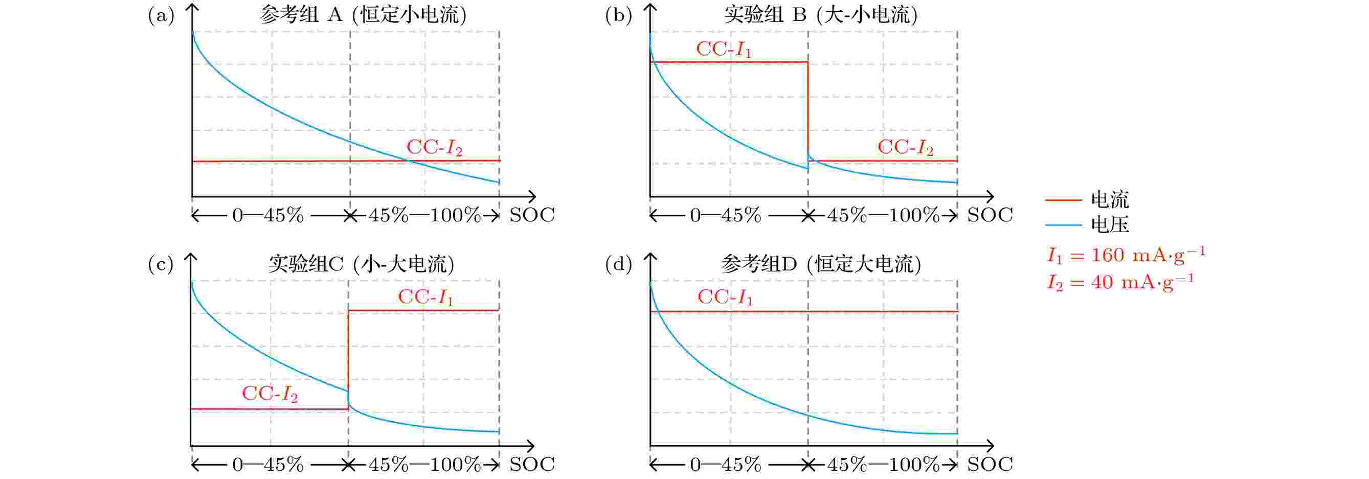
In this paper we conduct comprehensive experimental research and analyze the effect of charge-discharge modes on the performance of lithium storage. Four charge-discharge modes are designed, and the lithium storage performance experiments of the reduced graphene oxide electrode under different charge-discharge modes are carried out to analyze the effect mechanism of charge-discharge mode on lithium storage time and capacity from two aspects of electrode dynamic reaction performance and strain. The experimental results show that the shorter the lithium storage time of the electrode, the more the capacity loss under different charge-discharge modes. Comprehensive data analysis indicates that the charge transfer resistance, diffusion coefficient, overpotential and strain in the electrochemical process show non-linear and staged characteristics, resulting in the different lithium storage performances’ mechanism of different stages under different charge-discharge modes. Finally, “High current-low current” mode is proposed as a feasible optimization plan for charging and discharging. In the initial stage-I, the dual role of large electric field drive and concentration gradient drive enhances the migration and diffusion rate and shortens the lithium storage time; in the stage-II, the small current relieves local concentration accumulation and increases the amount of lithium inserted, thereby giving full play to the greatest advantage of current in each stage and balance the discrepancy between time and capacity. And this discussion provides certain guidance for designing and optimizing the fast charging technology.
CONDENSED MATTER: ELECTRONIC STRUCTURE, ELECTRICAL, MAGNETIC, AND OPTICAL PROPERTIES

2022, 71 (6): 067302.
doi:10.7498/aps.71.20211759
Abstract +
Compared with traditional inorganic ferroelectric materials, organic molecular ferroelectric materials possess many advantages, such as light weight, flexibility, no heavy metal atoms and low cost, and have received extensive attention for a long time. In recent years, atomic-thick two-dimensional (2D) inorganic ferroelectric materials have achieved breakthrough and attracted much attention. However, there are few reports on the design and research of two-dimensional organic ferroelectric materials. In this paper, we theoretically propose a 2D monolayer organic ferroelectric molecular crystal with the cyclobutene-1,2-dicarboxylic acid (CBDC) molecules as the building block based on density functional theory calculations. The bulk of CBDC molecular crystals clearly shows layered structure due to the chain-like arrangement of hydrogen bonds in crystal. It is found that the internal hydrogen bond chains give rise to the anisotropic cleavage energy values along different crystal planes of the CBDC molecular crystal bulk. Theoretical calculation suggests that the CBDC based 2D monolayer organic ferroelectric molecular crystal can be achieved by the mechanical/chemical peeling along the (102) crystal plane because of the lowest cleavage energy. It is predicted that the in-plane spontaneous polarization of the CBDC (102) molecular crystal monolayer is ~0.39 × 10⁻⁶μC/cm, which is comparable to those of some inorganic counterparts. Calculations also indicate that the CBDC (102) molecular crystal monolayer shows a high polarization reversal barrier and is sensitive to the external uniaxial stress. The CBDC (102) monolayer organic ferroelectric molecular crystal reveals high in-plane spontaneous polarization with polarization reversal barrier easily modulated by the interface strain engineering, thereby rendering it great potential in lightweight, metal-free and flexible ferroelectric devices.
2022, 71 (6): 067803.
doi:10.7498/aps.71.20211894
Abstract +
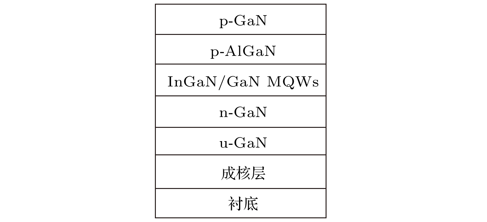
Optical band gap or band gap is an important characteristic parameter of semiconductor materials. In this study, several representative InGaN/GaN multiple quantum well structures are taken as the research objects, and the test conditions that need to be met for the luminescence measurement of the optical band gap of the InGaN well layer at a certain target temperature are discussed in depth. Since the InGaN well layer is a multi-element alloy and is subjected to stress from the GaN barrier layer, there exist not only impurity/defect-related non-radiation centers in the well layer, but also localized potential fluctuation induced by composition fluctuation and quantum confinement Stark effect (QCSE) induced by polarization field. Therefore, in order to obtain a more accurate optical band gap of the InGaN well layer, we propose the following test conditions that the luminescence measurement should meet at least, that is, the influence of the non-radiation centers, the localized centers and the QCSE on the emission process at the target temperature must be eliminated. Although these test conditions need to be further improved, it is expected that this test method can provide valuable guidance or ideas for measuring the semiconductor optical band gap.
2022, 71 (6): 067805.
doi:10.7498/aps.71.20211814
Abstract +
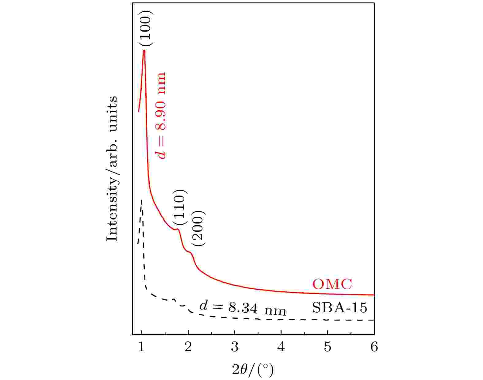
Owing to highly ordered two-dimensional hexagonal structure, large surface area, variable pore size, high thermal stability and especially the electron delocalization energy determined by its frame structure, SBA-15 catalysts have received more and more researchers’ attention. By using the structure-directing agent of P123 and the silicon source of TEOS, we synthesize ordered mesoporous silica SBA-15. At the same time, ordered mesoporous carbon OMC is succefully synthesized with the template of SBA-15. The small angle X-ray diffraction, high resolution transmission electron microscopy and N2adsorption-desorption measurements are conducted to verify the highly ordered pore structure and relatively high specific surface area of SBA-15 and OMC, and their average pore radius are about 7.5 nm and 3.3 nm, respectively. Positron lifetime spectrum of SBA-15 catalyst is composed of two longer lifetimes and two shorter lifetimes: two longer lifetimes
$ {\tau }_{3} $
and
$ {\tau }_{4} $
are the annihilation in micropore and large pore of positronium (Ps), are 7.5 ns and 106 ns. However, there is nearly no longer lifetime component in OMC, which indicates that there might exist the quenching or inhibiting of positronium by carbon material. To verify this guess, we synthesize the catalysts of OMC/SBA-15, OMC@SBA-15 and CuO@SBA-15 by the solid state reaction and the impregnation filling method. With the increasing of OMC and CuO content, both the o-Ps lifetime
$ {\tau }_{4} $
and its intensity
$ {I}_{4} $
of these three compounds decrease. The annihilation rate of o-Ps lifetime varying with OMC and CuO content can be better fitted by one or two straight lines, The values of reaction rate constant K in OMC/SBA-15, OMC@SBA-15 and CuO@SBA-15 are
$(2.39\pm $
$ 0.44)\times {10}^{7}~{\mathrm{s}}^{-1}$
/
$(6.65\pm 0.94)\times {10}^{6}~{\mathrm{s}}^{-1}$
,
$(2.28\pm 0.19)\times {10}^{7}~{\mathrm{s}}^{-1}$
, and
$(8.76\pm 0.47)\times {10}^{6}~{\mathrm{s}}^{-1},$
respectively. Therefore, our results indicate that there are quenching effect and inhibition effect among the carbon, the CuO and the positronium, which lead
$ {\tau }_{4} $
and
$ {I}_{4} $
to decrease, and positronium is also a probe for detecting the pore structure of porous material.
INTERDISCIPLINARY PHYSICS AND RELATED AREAS OF SCIENCE AND TECHNOLOGY
EDITOR'S SUGGESTION
2022, 71 (6): 068101.
doi:10.7498/aps.71.20211845
Abstract +
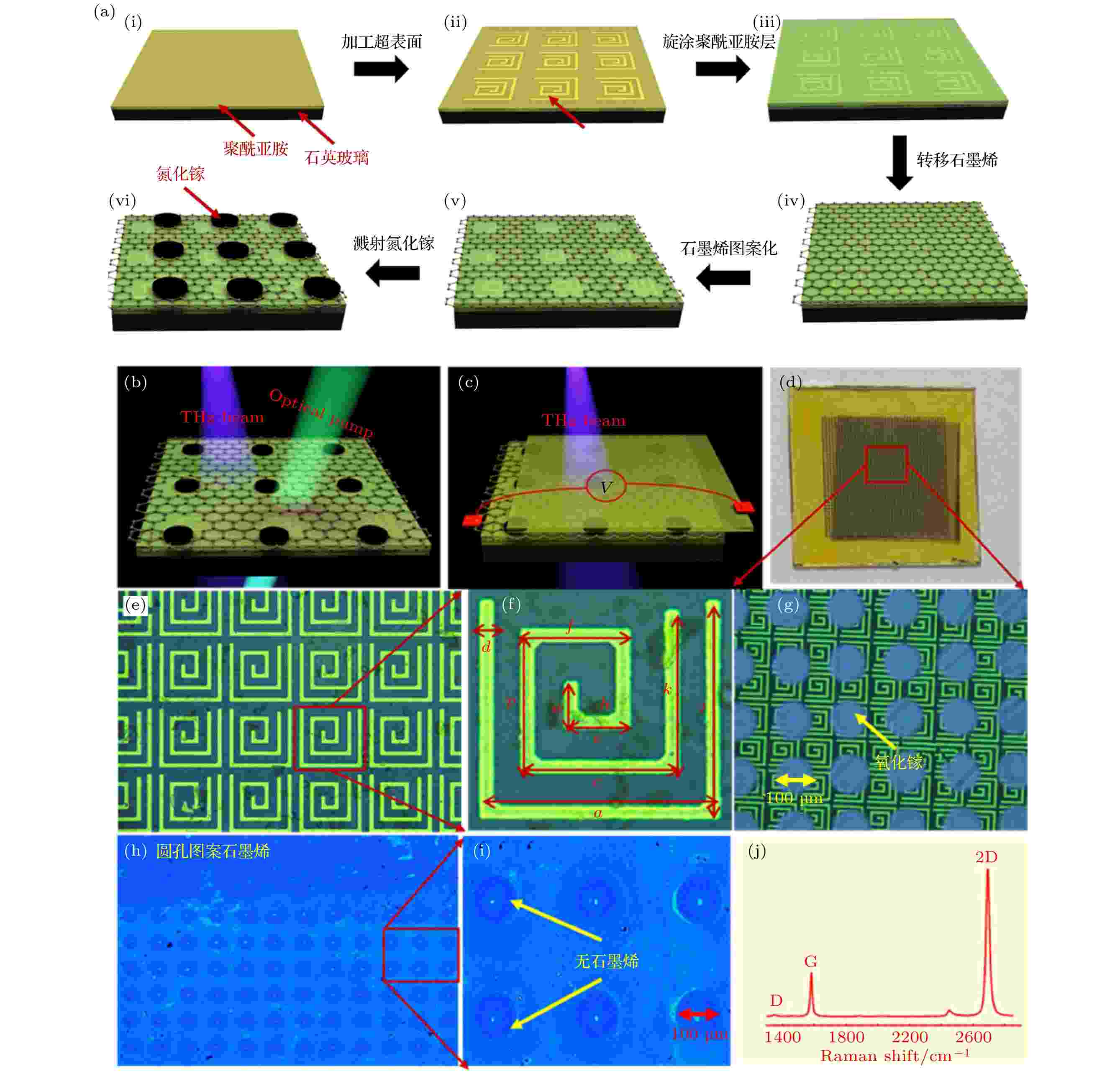
The development of terahertz (THz) technology is creating a demand for devices that can modulate THz beams. Here, we propose a novel THz modulator based on patterned graphene/gallium nitride Schottky diodes hybridized with metasurfaces. Ultrasensitive dynamic multidimensional THz modulation is achieved by changing the Schottky barrier of the heterojunction, shifting the Fermi level between the Dirac point, changing the conduction band and the valence of graphene via continuous-wave optical illumination or bias voltages. When the Fermi level is close to the Dirac point, the modulation is ultrasensitive to the external stimuli. Applying an optical power of 4.9–162.4 mW/cm2or a bias voltage of 0.5–7.0 V, the modulation depth initially increases, then decreases, and the phase difference linearly increases, therein the maximum modulation depth is 90%, and the maximum phase difference is 189°. In short, the proposed THz modulator has potential application in ultra-sensitive optical devices.
2022, 71 (6): 068501.
doi:10.7498/aps.71.20211655
Abstract +
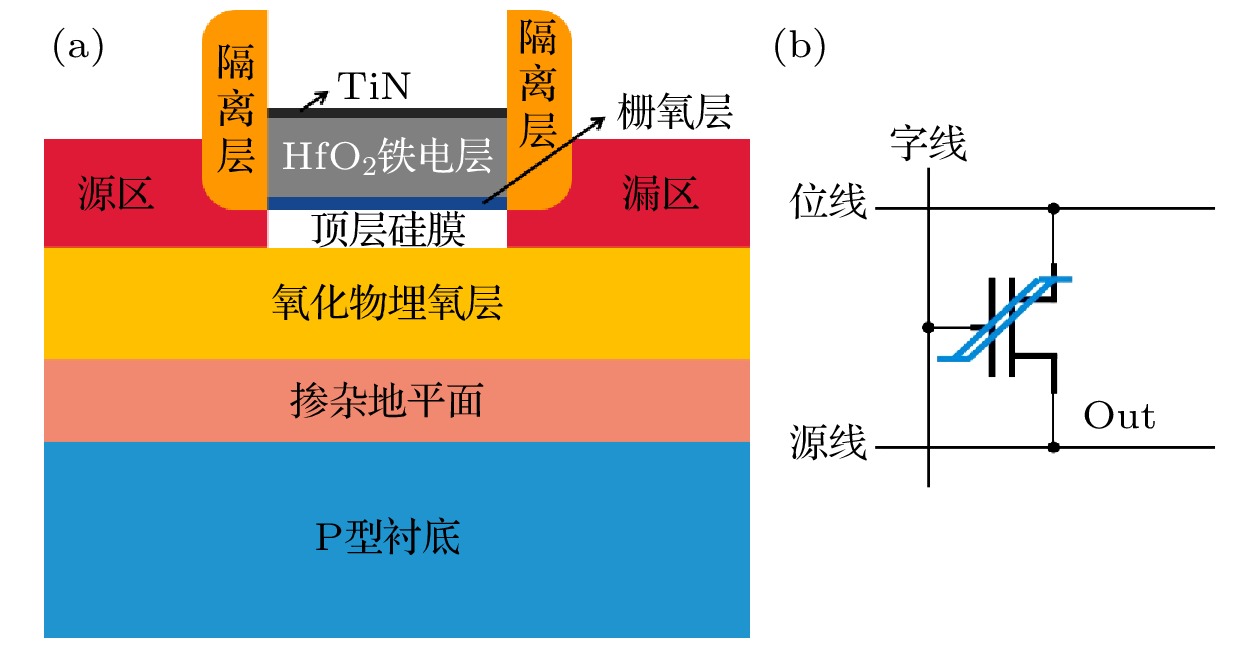
Ferroelectric field-effect transistor (FeFET) memory is currently a popular non-volatile memory. It has many advantages such as nonvolatility, better scalability, energy-efficient switching with non-destructive read-out and anti-radiation. To promote the application of FeFET in radiation environments, the single-event transient effect in HfO2-based fully-depleted silicon-on-insulator (FDSOI) FeFET memory cell is studied by technology computer aided design (TCAD) numerical simulation. The effects of different incident positions and angles of heavy ions and the drain bias voltage on the characteristics of the memory cell are analyzed. The results show that the corresponding polarization state in the HfO2ferroelectric layer will not reverse regardless of the change for the incident position of heavy ions, but the transient change of the output voltage for the memory cell will be affected. The most sensitive area is close to the drain-body junction area. Moreover, with the decrease of the ion incidence angle, the peak of output voltage for the memory cell increases. And the effect of the incident angle change is more obvious when reading data is “0” rather than “1”. The peak of output voltage for the memory cell is modulated by the drain bias voltage, and the modulation effect is more obvious when reading data is “1” rather than “0”. The above findings provide theoretical basis and guidance for the anti-single event design of the FDSOI FeFET memory cell.
2022, 71 (6): 068901.
doi:10.7498/aps.71.20211621
Abstract +
In many complex networks, such as communication networks, power grids, and transportation networks, the main task is load transmission from sources to destinations. Therefore, the transmission throughput is a very important indicator to measure the network performance, and improving the throughput becomes one of the hotspots in the research of these complex networks. Many researchers have proposed different routing algorithms to improve the network throughput. However, few of them considered the spatial location of nodes in the network. Indeed, many real-world networks can be modeled by spatial networks, where the spatial location of nodes plays a vital role in determining the structure and dynamic behaviors of such networks. Specifically, when the locations of nodes are considered, each link has a length. And the shortest path may have different meaning. Traditionally, the shortest path indicates the path which passes the least number of links from source to destination, or the least number of hops. However, when the length of link is taken into account, the least number of links does not mean the least summation of link lengths along the path. The latter can be called the shortest path length. To this end, we proposes an efficient routing strategy for spatial networks based on the shortest path length in this work. In order to test the effectiveness of the algorithm, the network throughput
${R}_{\rm c}$
is used, at which the network changes from a free flow state to a congestion state, to measure the performance of the network. Simulations of homogeneous and heterogeneous spatial networks show that compared with the traditional least number of hops routing strategy, the routing algorithm based on the shortest path length proposed in this paper can effectively improve the throughput of the network. The routing algorithm proposed in this paper can be applied to many real-world spatial networks for improving their performances.


