Vol. 69, No. 19 (2020)
2020-10-05
INVITED REVIEW
INVITED REVIEW
2020, 69 (19): 190701.
doi:10.7498/aps.69.20200788
Abstract +
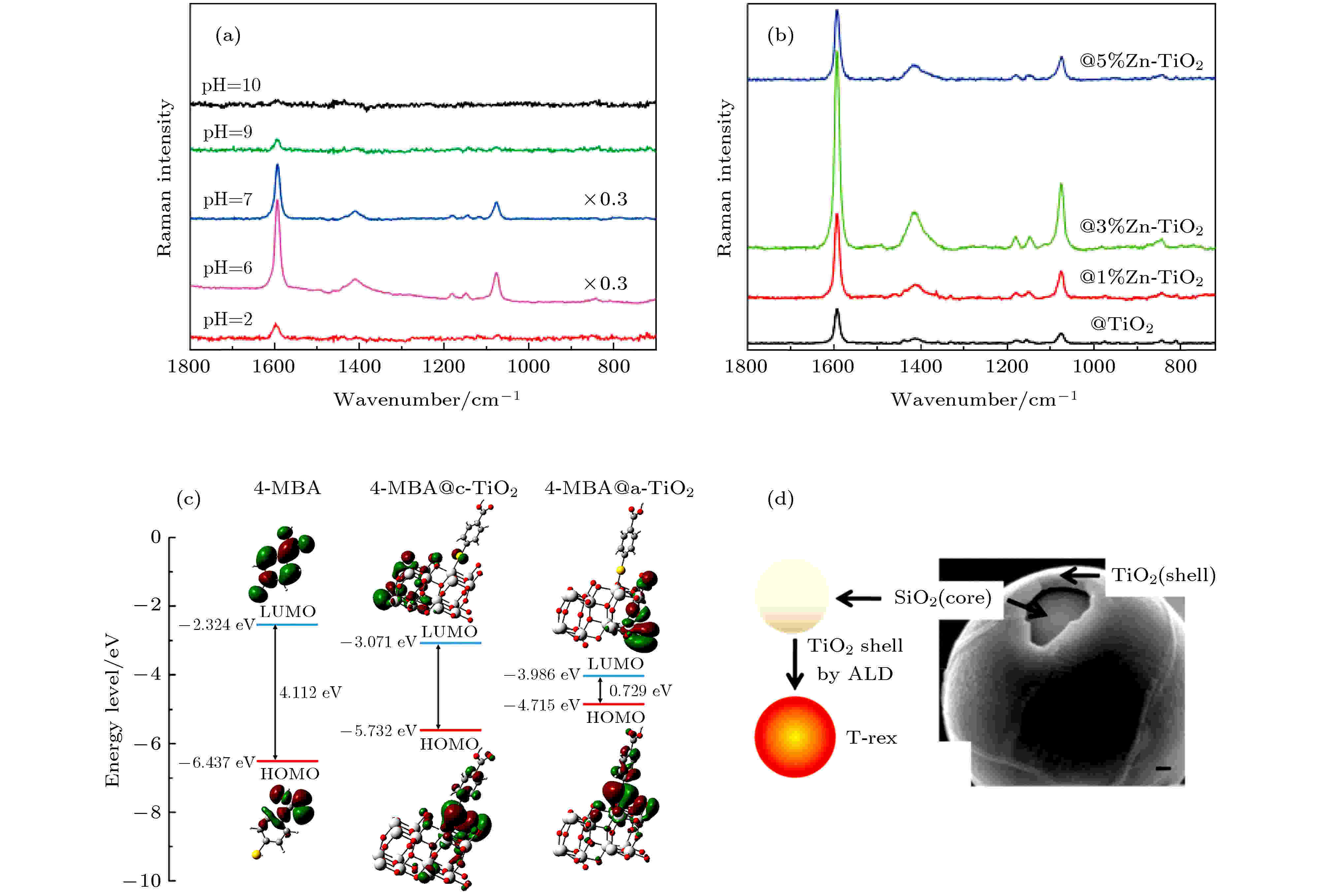
Surface-enhanced Raman scattering (SERS) is of great importance in analytical science, the noble-metal such as gold and silver are widely used in SERS research and applications. However, noble-metal based substrates are hampered in practical application. As for comparison, the Non-noble metal especially the semiconductor materials are the emerging SERS research frontier. Non-noble metal (such as C, Ti, Zn, Cu, Mo, W, etc.) nanomaterials based SERS substrate have been widely studied and applied due to their superior stability, selectivity, biocompatibility and low cost comparing to noble metal materials. As the chemical enhancement dominate its total SERS signals, it also provides an ideal platform for the investigation of chemical enhancement mechanism. In this review, we explored the development of non-noble metal SERS substrates, focusing on its enhancement mechanism and SERS performance of different materials as well as the future development direction.
INVITED REVIEW
2020, 69 (19): 196401.
doi:10.7498/aps.69.20200707
Abstract +
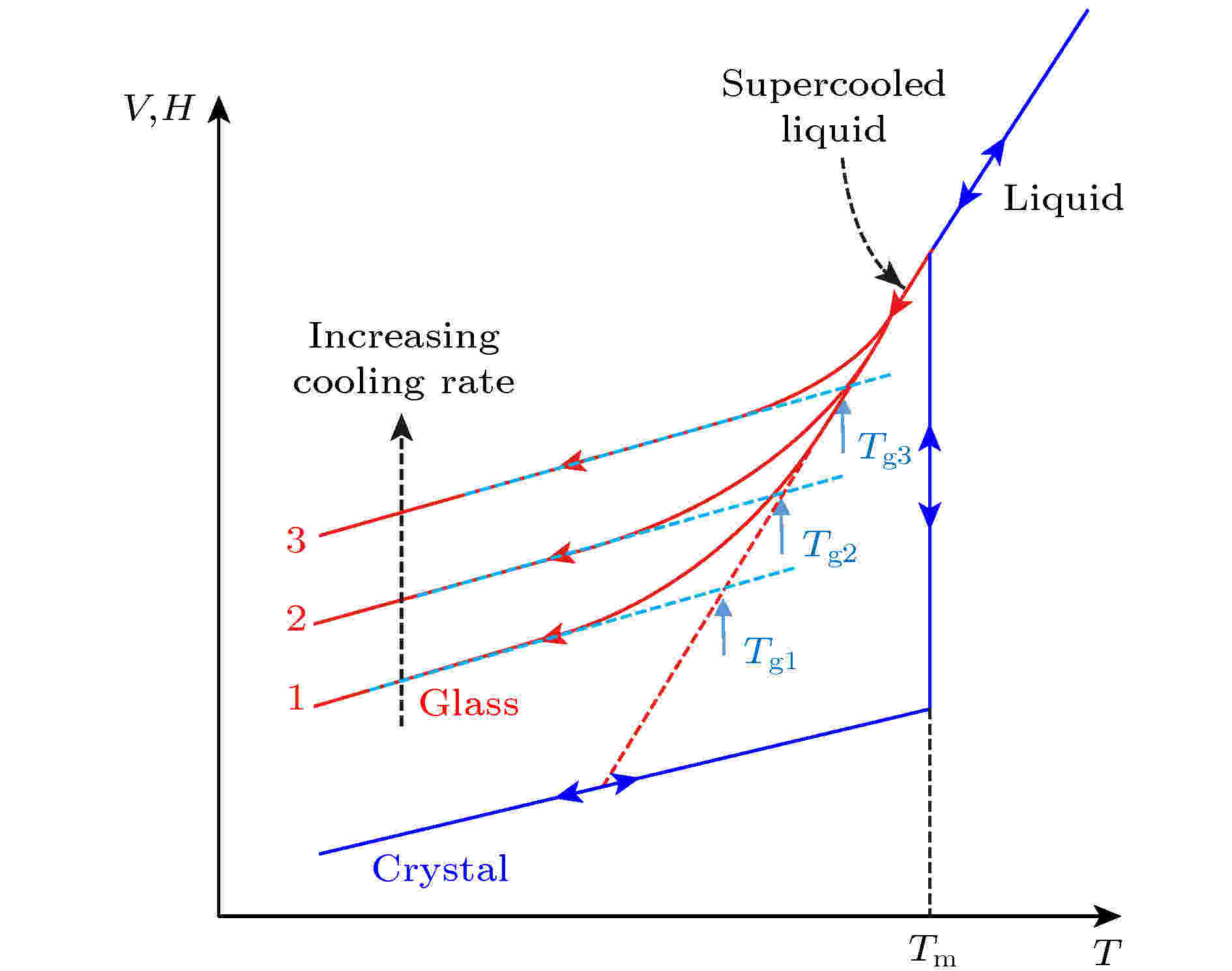
Glass formation thermodynamics usually concerns the liquid-crystal Gibbs free energy difference. But, in practice, its efficiency in predicting the occurrence of the glass transition of materials and guiding the composition design is quite quantitative. In particular, it remains to be clarified to understand the relationship between and the contributions to the two fundamental quantities of enthalpy and entropy involved herein. In this paper, we study the relation between the enthalpy and the entropy involved in glass formation of various materials, and find that they are strongly correlated with each other. Theoretical and experimental analyses indicate the intrinsic correlation of the entropy of fusion with other key parameters associated with glass formation like melting viscosity and enthalpy of mixing, which confirms the close relation between the entropy of fusion and glass formation. Close inspection finds that the low entropy of fusion benefits the glass formation. Owing to the fact that the two glass-formation key variables of viscosity and enthalpy can be addressed by the entropy of fusion, we propose that the entropy of fusion be able to serve as a representative thermodynamic quantity to understand the glass formation in materials. The reliability in understanding the glass formation in terms of entropy of fusion is further verified. The studies provide a new reference for developing the glass formation thermodynamics.
INVITED REVIEW
2020, 69 (19): 196602.
doi:10.7498/aps.69.20200709
Abstract +
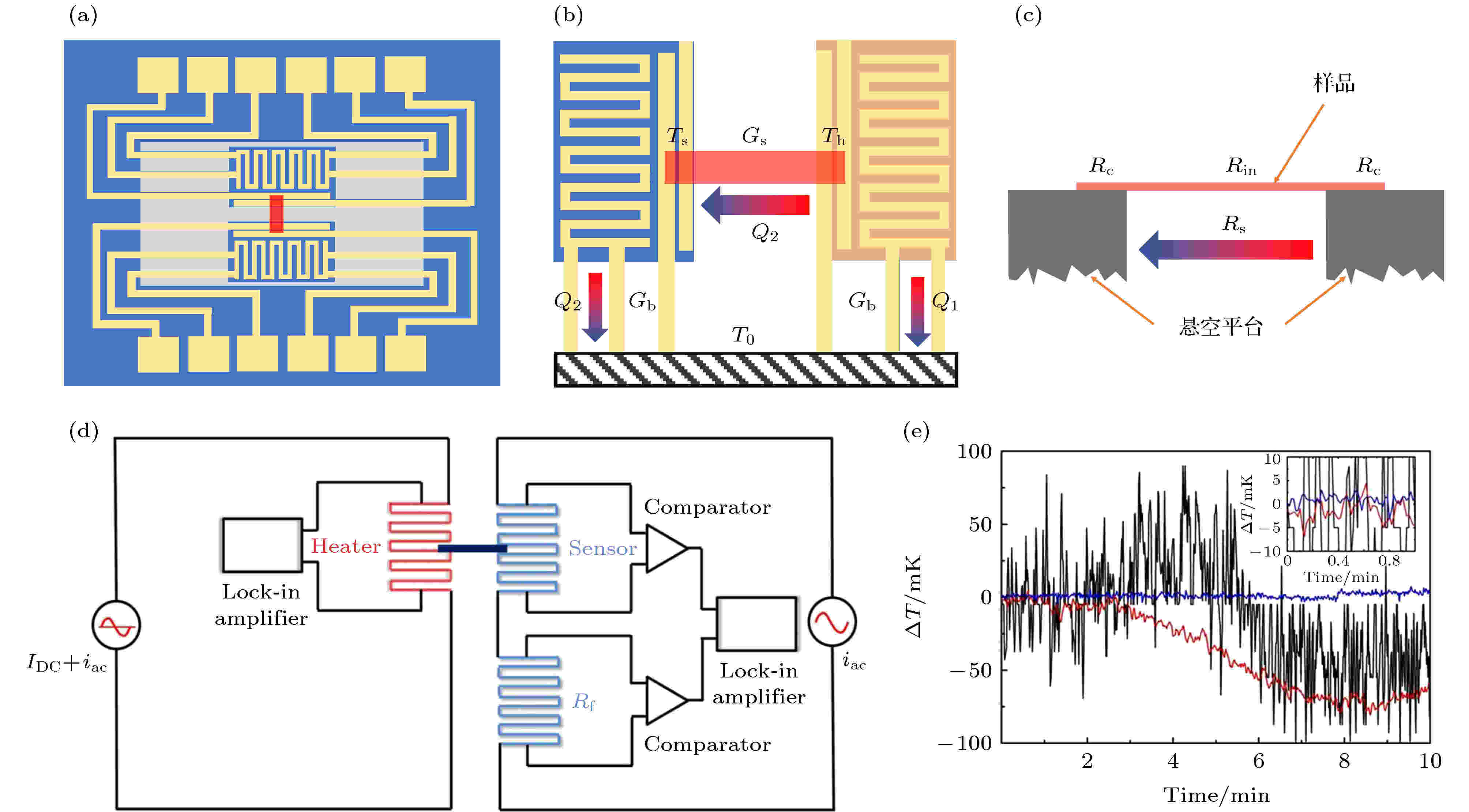
The two-dimensional (2D) materials represented by graphene and boron nitride provide an excellent platform for the study of thermal conduction and the interfacial thermal resistance in low-dimensional system. Recent studies recover exotic physics behind the novel thermal transport properties of 2D materials, such as length effect, dimensional effect, isotopic effect, anisotropic effect, etc. In this review, we introduce the recent progress of thermal properties in 2D materials in the last decade. The principle and development of thermal conduction measurement technologies used in 2D materials are introduced, followed by the experimental progress of thermal conduction and interfacial thermal resistance. Special attention is paid to the abnormal thermal transport and relevant physical problems. Finally, we present thermal management and heat dissipation in 2D electronic devices, summarize and point out the problems and bottlenecks, and forecast the future research directions and foregrounds.
GENERAL

A simple protocol for measuring device independent quantum key distribution based on hybrid encoding
2020, 69 (19): 190301.
doi:10.7498/aps.69.20200162
Abstract +
Quantum key distribution technology refers to a method to share keys between communication parties by transmitting quantum states in public channels. Although unconditional security is the main advantage of QKD, its application prospect has been controversial in practical implementation due to the potential security risks caused by device imperfections. Fortunately, the measurement device independent quantum key distribution protocol removes the vulnerability of all measurement devices and greatly improves the practical security of the quantum key distribution system. However, the security key rate of this protocol is still lower than that of other quantum key distribution protocols. At present, using high-dimensional coding to improve the performance of the quantum key distribution protocol has been proved in theory and experiment, and recently, it has been proposed to use high-dimensional coding to improve the performance of measurement device independent quantum key distribution protocol, but because these protocols have higher requirements for the laboratory equipment performance, that the high-dimensional encoding is applied to the aforementioned protocol still has many difficulties in practical application. In this paper, we propose a hybrid coding based on the polarization and two-degree phase of freedom measurement device independent quantum key distribution protocol. In the first place in an ideal case, we introduce in detail the protocol decoding rules, then introduce 4intensity decoy-state method to solve the problem of actual light source multiphoton, in addition we also consider the statistical fluctuation effect under the condition of limited code length, channel loss, actual dark count of single photon detector and detection efficiency problem. Finally, the optimal security code rate and its corresponding optimal parameters are obtained by full parameter optimization method, And the numerical simulation results show that the security key rate of this protocol is increased by 50% by considering the practical implementation. We point out that compared with other measurement device independent quantum key distribution protocol, the proposed agreement requires local users only to have a phase encoding device and a polarization coding device, and 4 single photon detectors for detecting side. The proposed device can use the existing experimental condition, beyond that, compared with the time encoding based high dimensional measurement device independent quantum key distribution protocol, the proposed protocol possesses the advantage that the rate of system security key can be increased without increasing the repetition frequency of users. It is proved that this protocol has great application value in the future field of quantum communication, especially, in the field of quantum network communication.

2020, 69 (19): 190302.
doi:10.7498/aps.69.20200244
Abstract +
Most of the classical designated verifier signature schemes are insecure against quantum adversary. In this paper, a quantum signature scheme for the designated verifier is proposed. In our scheme, during the initialization phase, the partners share secret keys by performing the quantum key distribution protocol. On the other hand, by performing the quantum direct communication protocol, the key generator center shares secret keys with the signer and the designated verifier, respectively. The key generator center generates a particle sequence of Bell state and distributes the particles between the signer and the designated verifier. During the signature generation phase, the signer encrypts the particle sequence by the secret keys and Hardmard operators. After that, the signer performs the controlled unitary operations on the encrypted particle sequence so as to generate the quantum signature. The designated verifier can simulate the quantum signature by performing the same symmetric signing steps as that performed by the original signer. Hence, the quantum signature signed by the true signer is the same as the one simulated by the receiver, which makes our scheme possess the designated properties. During the signature verification phase, the designated verifier performs the controlled unitary operations on the quantum signature and obtains the quantum ciphertexts. After that, the designated verifier decrypts the quantum ciphertexts by the symmetric secret keys and Hardmard operators so that the quantum signature can be verified. Our signature is secure against forgery attack, inter-resending attacks and Trojan horse attack. Because the trace distance between the density operators of different quantum signatures is zero, the information-theoretical security of our quantum signature scheme can be proved. The unconditionally secure quantum key distribution protocol and the one-time pad encryption algorithm can guarantee the security of the secret keys shared by the partners. What is more, the security assumption about the key generation center is weak. That is, it is not necessary to assume that the key generation center should be fully trusted. On the other hand, in our scheme, the quantum one-way function is not used. To generate a quantum signature, the signer need not prepare for entangled particle sequence. To verify a quantum signature, the verifier need not apply any state comparison to the received particles. The qubit efficiency is 100%. Therefore, our scheme has the advantages in the security and efficiency over the other quantum signature schemes for the designated verifier.

2020, 69 (19): 190601.
doi:10.7498/aps.69.20200281
Abstract +
Laser Doppler vibrometer can measure the displacement, velocity, acceleration and other parameters of vibration target. It has the characteristics of non-contact, high precision and long distance. So, it has a great advantage for the vibration measurement in a special working environment, where the target is light and thin, hard to contact, hard to approach. Laser heterodyne interferometry is an important means of detecting the micro vibration. With the development of micro vibration application, the sensitivity of phase measurement is highly required. Traditionally, there are several ways of improving the measurement sensitivity, such as optimizing the heterodyne interference scheme, improving the phase reconstruction algorithm and reducing the noise of key devices and so on. However, based on the analysis of the influence of stray light in the system, it is found that the controllable multi-beam interference can greatly improve the detection capability of the system. Therefore, a phase enhancement technique of multi-beam hybrid interference is proposed to meet the needs of high sensitivity detection of micro vibration. In this paper the physical mechanism and boundary conditions of phase enhancement are investigated in detail, and the quantitative relationship between the boundary conditions and phase enhancement is also analyzed thereby providing a technical reference for the enhancement detection of micro vibration targets. Through the numerical simulation and experimental verification, the following boundary conditions are obtained: the initial phase difference between the correction light and the signal light is π rad and the closer the power values of the two beams, the greater the enhancement effect of the demodulation phase is. The power difference between the two beams designed in the experiment is 1%, which means that detection capability is enhanced by 146 times. It has great application value in the high sensitivity measurement of micro vibration objects. This technology can also enhance the detection capability of heterodyne interference measurement system without changing the existing device index or phase demodulation algorithm.
NUCLEAR PHYSICS
2020, 69 (19): 192401.
doi:10.7498/aps.69.20200064
Abstract +
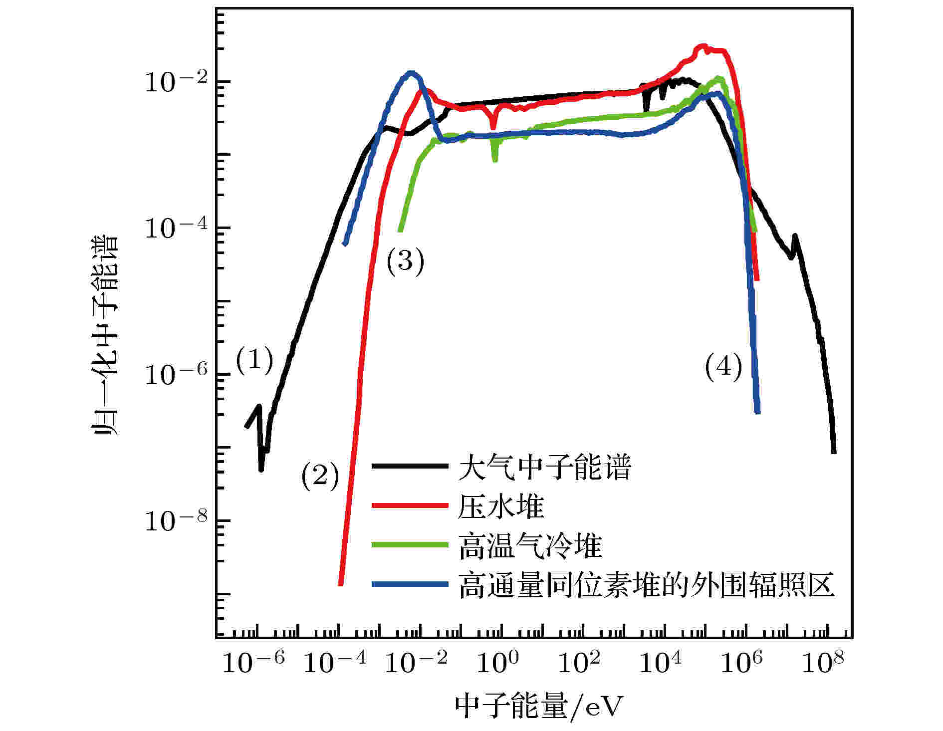
Gallium nitride (GaN), one of the third-generation wide-bandgap semiconductors, offers significant application for advanced electronic devices utilized in neutron irradiation environments, like the defense, space, and aerospace, etc. In these applications, neutron irradiation-induced defects affect the properties of GaN and eventually degrade the performance of devices. In this work, neutron transport process in GaN is simulated by using the Monte Carlo-based code, Geant4 toolkit under four different irradiation conditions, e.g. high flux isotope reactor, high temperature gas-cooled reactor, pressurized water reactor, and atmospheric neutron irradiation. The energy spectra of primary knock-on atoms (PKA) in GaN and the corresponding weighted spectra under those irradiation conditions are analyzed. It is found that there is one unusual “peak” at around 0.58 MeV in the Primary recoil spectrum, regardless of the irradiation conditions. This peak is attributed to the neutron reaction of hydrogen nucleus, i.e., (n, p). Because of the remarkable (n,p) reaction cross-section of low-energy neutron, the intensity of this peak is related to the ratio of low-energy neutron to the total neutron spectrum. By comparing these PKA energy spectra in GaN, we can see that the PKA energy spectrum created under atmospheric neutron irradiation is similar to that in the high flux isotopic reactor. Specifically, the energy distribution of PKA is wide, and the magnitude of energy is lower than those under fission neutron irradiation conditions. In combination with the effects of nuclear reaction products on electrical properties, the high flux isotopic reactor is more suitable for simulating the irradiation of GaN in an atmospheric neutron energy spectrum environment. These above results can provide not only some insights into the evaluation of the degradation of GaN-based electronic devices under neutron irradiation, but also dataset for the study of radiation damage effect of GaN in simulated neutron environment.
ATOMIC AND MOLECULAR PHYSICS
2020, 69 (19): 193101.
doi:10.7498/aps.69.20200756
Abstract +
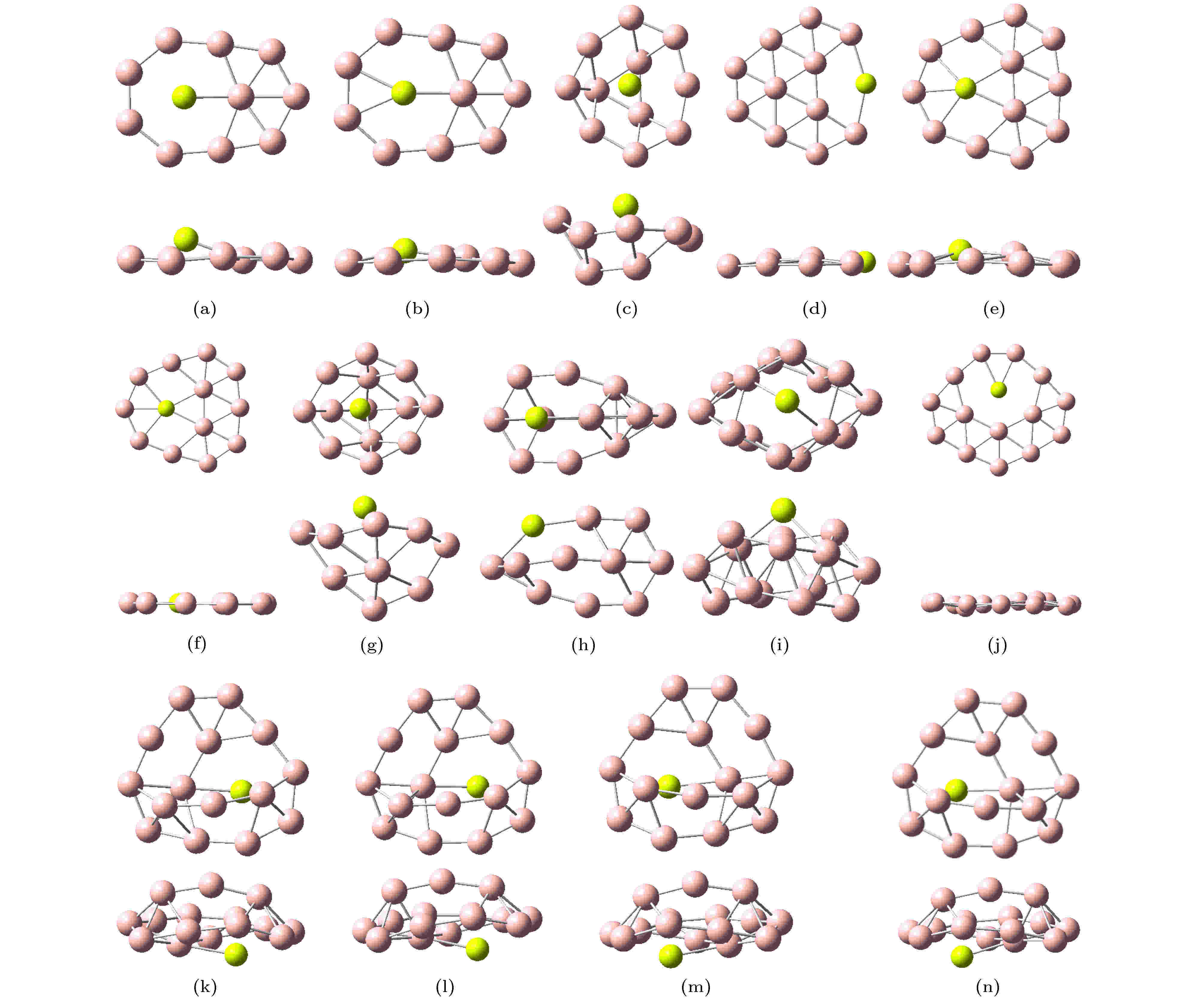
A theoretical study of geometrical structures and electronic properties of Be atom doped boron clusters BeB
$ _n^{0/-} $
(n= 10–15) is performed using the CALYPSO approach for the global minimum search followed by density functional theory calculations. It is found that the global minima obtained for the BeB
$ _{10}^{0/-} $
, BeB
$ _{11}^{-} $
, BeB
$ _{12}^{0/-} $
, and BeB
$ _{14}^{-} $
clusters correspond to the quasi-planar or planar structures. However, the global minima obtained for the BeB11, BeB13, BeB
$ _{13}^{-} $
, BeB14clusters correspond to the half-sandwich, cone, cage, squashed tubular structures, respectively. Interestingly, both the neutral and anionic BeB
$ _{15}^{0/-} $
clusters have the axially chiral isomers which are chiral with degenerate enantiomers. Natural population analyses reveal that partial charge on Be atom transfer to boron atoms. The average binding energy values of BeB
$ _n^{0/-} $
(n= 10–15) indicate that anionic clusters are overall more stable than the corresponding neutral ones, and both neutral and anionic clusters show the same trend that the stability increases gradually with the increase of B atoms number n. Chemical bonding analyses of closed-shell BeB10, BeB
$ _{11}^{-} $
, BeB12clusters reveal that the σ bonds stabilize whole molecular skeleton, and delocalized π bonds render the structure more stable. Furthermore, the three quasi-planar closed-shell clusters possess 3 delocalized π bonds, which quite surprisingly follow the 4m+ 2 Hückel rule for aromaticity. Average polarizability of single atom for each quasi-planar or planar structure is larger than other structures, it indicates that quasi-planar or planar structure has stronger electron delocalization. Specifically, BeB
$ _{13}^{-} $
and BeB
$ _{14}^{-} $
with large first static hyperpolarizability can lead to the remarkable NLO response. The calculated spectra indicate that BeB
$ _n^{0/-} $
(n= 10–15) have the meaningful characteristic peaks which can be compared with future experimental values. Our work enriches the database of geometrical structures of doped boron clusters and can provide much insight into the new doped boron clusters.
EDITOR'S SUGGESTION
2020, 69 (19): 193102.
doi:10.7498/aps.69.20200651
Abstract +
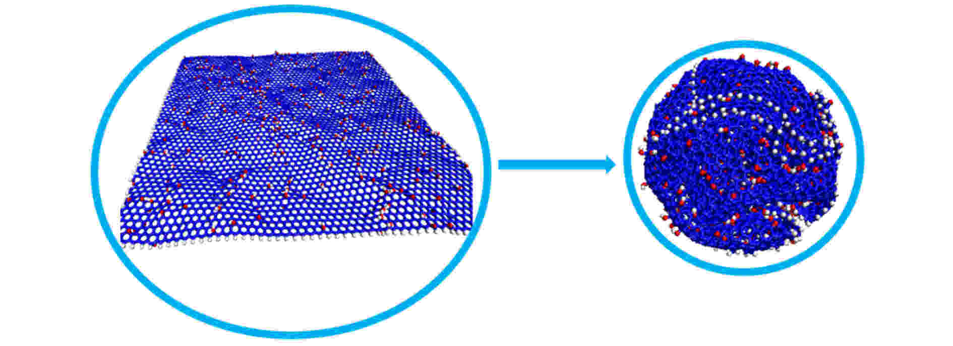
Graphene has a wide range of applications in the fields of electricity, chemistry, biomedicine, and lubrication. But the strong van der Waals interaction between graphene sheets makes it easy to aggregate in preparation process, difficult to produce and put into practical applcation on a large-scale. There are many methods to prevent the graphene sheets from aggregating, such as reducing the size of sheets, adjusting the interaction between solvent and graphene, and using dispersant. Another possible method is to turn the sheet graphene into a three-dimensional structure like the crumpled paper. Compared with sheet graphene, the crumpled graphene ball has excellent aggregation-resistant. The current research on crumpled graphene ball mainly focuses on the effect of the initial structure of graphene sheet on the structure stability of the crumpled ball, but rarely involves the effect of functional groups. In this paper, ReaxFF molecular dynamics is used to simulate the crumpling process of graphene oxide sheet. The effect of functional groups (hydroxyl, epoxy) on the crumpling behavior and the stability of the crumpled ball of graphene oxide are studied. Graphene sheet oxidized by hydroxyl exhibits a push-up crumpling behavior. Graphene sheet oxidized by epoxy exhibits a layer-to-layer fitted crumpling behavior. Different crumpling behavior will lead to the difference in final crumpled ball structure. By analyzing the relationship between the atomic level potential energy incremental distribution and the distribution of broken and formed C—C bonds, we find that the broken and formed C—C bonds mainly occur in areas with a large degree of deformation, and the epoxy group has a stronger weakening effect on the C—C bond connected to it than the hydroxyl group. The release process of graphene oxide crumpled ball is simulated to study its structural stability. The stability of graphene oxide crumpled ball depends on the number of the broken and formed C—C bonds, that is, the more the number of broken and formed C—C bonds, the more stable the structure is, and under the same oxidation rate, the stability of the crumpled ball structure increases with the proportion of epoxy groups increasing. This study shows that the stability of graphene oxide crumpled ball structure can be controlled by changing the relative proportion of functional groups.

Experimental realization of Mott insulator of ultracold87Rb atoms in two-dimensional optical lattice
2020, 69 (19): 193201.
doi:10.7498/aps.69.20200513
Abstract +
Quantum phase transition of ultracold atomic gas is one of the core contents in the study of quantum correlational many-body systems. In this paper, two-dimensional (2D) optical lattices are generated by a single fold retroreflected laser beam, and this scheme is used to experimentally design and implement the 2D optical lattice of double wells suitable for isolating and manipulating an array of individual pairs of atoms and predict a topological semimetal in the high orbital bands in this 2D lattice. Two types of optical lattice structures are produced by controlling the laser polarization. One type is the usual 2D optical lattice, which is formed by two independent one-dimensional(1D) optical lattices in two directions and named in-plane lattice, and the other type is the lattice that is formed by the interference between two one-dimensional optical lattices in two directions and called out-plane lattice. When87Rb BEC (Bose-Einstein condensation) is loaded into the 2D optical lattice, the quantum phase transition between superfluid state and Mott insulator state is observed by controlling the tunneling and in-site interaction. And the phase transition from superfluid state to Mott insulator is judged by observing whether there are interferential lattice points in momentum space. The lattice depths of two cases can be calibrated by Kapitza-Dirac scattering in the ultracold atomic experiment through the time-of-flight absorption imaging. In the in-plane optical lattice, some incorrect points appear in the 45° direction, because the linear polarization degree of beam is impure after being reflected by mirrors and two direction of beam are not completely orthogonal to each other. It is obvious that the two cases have different phase transition points, which is due mainly to the difference in structure. For the in-plane lattice, there are two independent 1D optical lattices, and for the out-plane lattice, the two direction beams mutually interfere with each other, therefore, two optical lattices are not independent of each other. The atoms come back to BEC by reducing the potentials of optical lattice to zero; the temperature of system is slightly higher, because of the jitter of the light lattice. The different behaviors of quantum phase transition are analyzed for two types of optical lattices. This work will provide a platform for the future study of large spin system and strong correlation physics in optical lattices.
ELECTROMAGNETISM, OPTICS, ACOUSTICS, HEAT TRANSFER, CLASSICAL MECHANICS, AND FLUID DYNAMICS

2020, 69 (19): 194101.
doi:10.7498/aps.69.20200501
Abstract +
Generating low-frequency electromagnetic waves based on high-frequency antenna and illuminating targets with multi-band signals can be an effect way that can not only reduce the physical dimension of a low frequency antenna, but also improve the performance of radar detection. Combining the electromagnetic wave doppler effect principle and the array antenna architecture, a method of generating a low-frequency signal around the illuminated target is proposed based on the controlling of array antenna parameters, including array radiation element signal timing, phase and element spacing. The principles of array parameter design are described. Composite signals are simulated respectively under two typical geometric relationships between targets and array antenna, target located along the array direction and in the direction of 45° scanning angle. The peak sidelobe ratio (PSLR) and integral sidelobe ratio (ISLR) are used to evaluate the quality of the composite signals. Aiming at practical applications, the effects of array element spacing error, phase error and target location error on the composite signal are simulated and analyzed. Under the condition of sparse uniform array, the influence of the radiation element spacing on the composite signal is analyzed. The simulation results show that the harmonic components of the composite signal increase with the radiating element spacing error and phase error growing.
EDITOR'S SUGGESTION
2020, 69 (19): 194201.
doi:10.7498/aps.69.20200532
Abstract +

2020, 69 (19): 194202.
doi:10.7498/aps.69.20200750
Abstract +
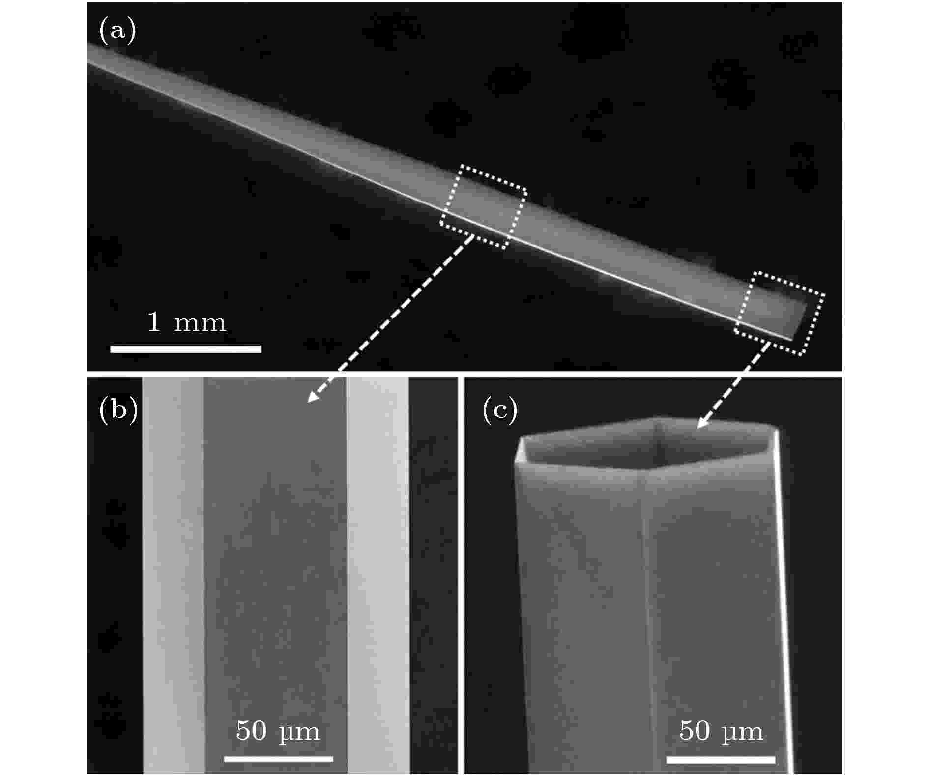
The integration of fiber with graphene has greatly expanded the two-dimensional functional materials in the field of photonics research. However, the growth method by using chemical vapor deposition with metal catalytic substrateis limited to the fabrication of a graphene-fiber composite due to inevitably transferring graphene flakes onto the optical fiber surface. In order to fully achieve the interaction between light and graphene material, optical fibers have to be treated with special structure, which greatly damages the fiber structure, resulting in inefficient and harmful manufacturing strategy for the mass production. In this paper, a graphene-photonic crystal fiber (G-PCF) composite is prepared by atmospheric chemical vapor deposition (APCVD), which can directly grow monolayer and multi-layer graphene into the air-hole of photonic crystal fiber. Furthermore, we randomly break a G-PCF and then conduct an electron microscope (SEM) test at the fractured section. It is obvious that a tube-like graphene protruding out of one hole in the fractured area of the G-PCF is observed, thus further demonstrating that a monolayer graphene is grown on the inner hole walls of the PCF as shown in
Fig. 2
. By changing the process parameters such as growth temperature, duration and gas flow rate of carbon source, the law of the influence of different parameters on the graphene layers is explored. In addition, the uniformity of graphene and defects in the graphene-photonic crystal fiber(G-PCF) are experimentally analyzed. As illustrated in
Fig. 7
, a 4-cm-long uniform graphene-photonic crystal fiber sample is achieved by controlling the gas flow rate, growth time and the growth temperature. The APCVD method of directly growing graphene onto the inner hole walls of the PCF is simple and effective. The flexible structure and optical control enable the G-PCF to have great potential applications in all-optical devices and photonics. The development of high-quality graphene synthesis and opto-electronics technology ensures its compatibility with the integrated electronics platform and existing optical fiber systems. Moreover, our results will pave the way for 2Dmaterials and optical fiber applications, providing a new idea for the application of graphene to the integration of all-optical fibers.

2020, 69 (19): 194301.
doi:10.7498/aps.69.20200414
Abstract +
2020, 69 (19): 194701.
doi:10.7498/aps.69.20200549
Abstract +
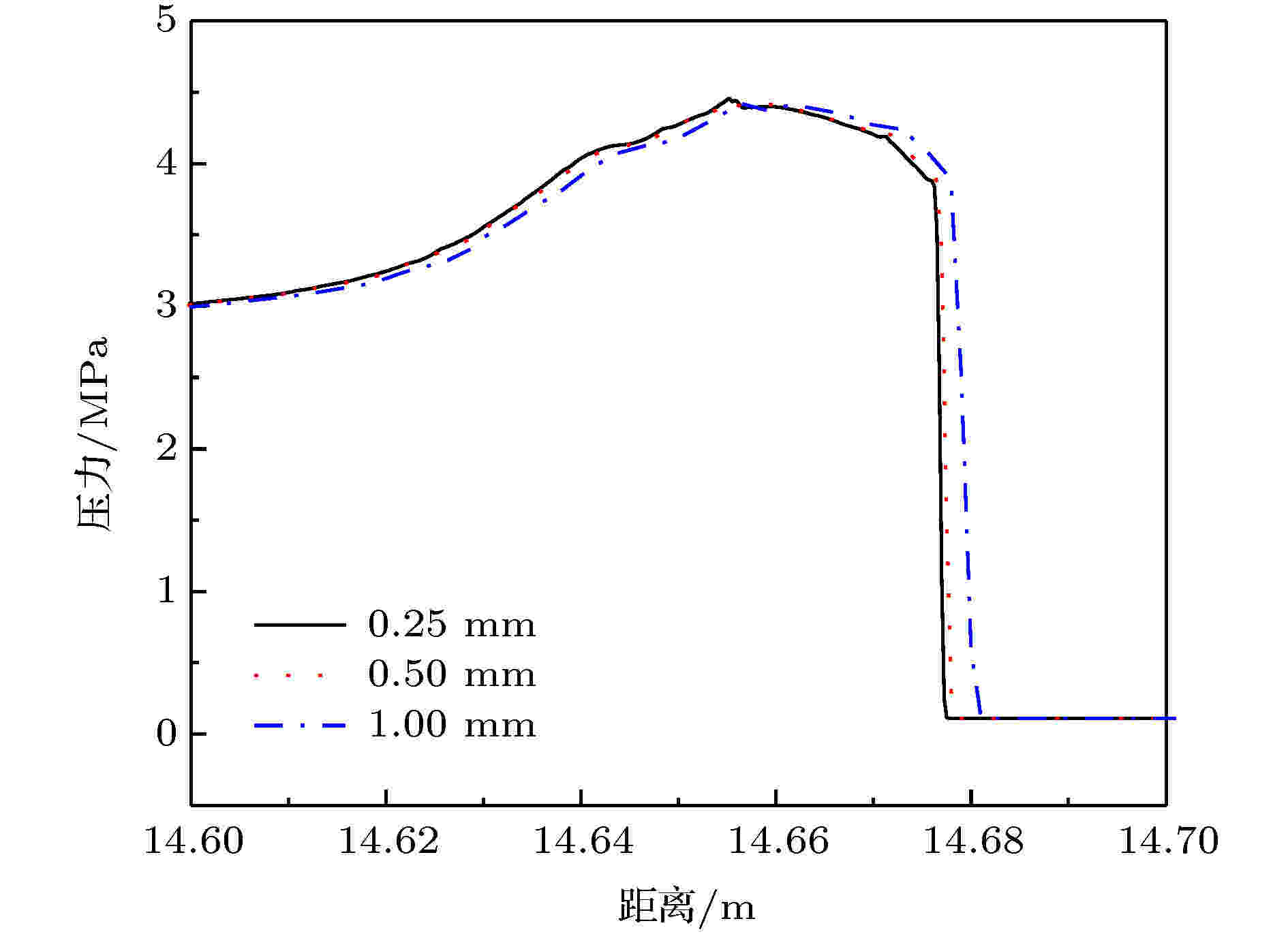
In this paper, a one-dimensional unsteady model is established for the detonation of magnesium particle-air mixture. Through numerical simulation, the influences of the loss caused by the side wall of the detonation tube, the diameter of the magnesium particles, the initial equivalent ratio of the magnesium particles, and the deposition process on the surface of the particles, and the ignition energy on the structure and development of the detonation wave and the distribution of the flow field parameters inside the detonation wave are obtained. The studies show that there appear oscillations during the propagation of the fully developed one-dimensional unsteady detonation wave of magnesium particle-air mixture, but the amplitude is less than 1 m/s. Considering the loss of the wall, the pressure and temperature inside the detonation wave decrease with the inner diameter of the detonation tube decreasing, thus leading the propagation velocity and the thickness of the detonation wave decreasing. In the case without the wall loss, as the initial particle size increases, the detonation wave velocity remains unchanged, and the detonation wave thickness monotonically increases. With the wall loss taken into consideration, the stable velocity and thickness of detonation wave are lower than without considering the wall loss under the same initial conditions. Both the difference between the velocities and the difference between thickness values under the conditions with and without considering the wall loss increase as initial particle size increases. The detonation wave thickness with a double-size-distribution initial particle size is more than that with an equivalent single-size-distribution. Meanwhile the stable propagation velocity of the former is less than that of the latter. In the range of initial particle equivalent ratio of 0.5–2, as the initial equivalent ratio increases, the stable velocity of ideal detonation wave first increases and then decreases, and the thickness of the detonation wave first decreases and then increases. Considering the loss of the wall, with the increase of the initial equivalence ratio, the stable velocity of detonation wave first decreases and then increases and the thickness of the detonation wave monotonically decreases. When the initial equivalence ratio of the initial particles is in a lower range (0.337–0.382), the melting of MgO occurs near the CJ plane. As a result, the melting process of MgO has no significant effect on the stability of the detonation wave propagation, but has a greater influence on the structure of the detonation wave: when the initial equivalence ratio is lower in the above range, MgO in the detonation wave is partially melted and then re-solidified. When the initial equivalence ratio is higher in the above range, the MgO at the CJ plane is still in the melting process, and there is a low-strength secondary compression process in the detonation wave. Considering the fact that the combustion products are deposited on the particle surface, the detonation wave velocity increases while the corresponding thickness of the detonation wave remains almost unchanged with the increase of the deposition rate. The parameters of the ignition region have no influence on the final stable propagation state of the detonation wave, but will affect the development process of the detonation wave. Selecting appropriate paraneters of ignition zone can shorten the distance of denotation wave reaching to the steady propagation.
PHYSICS OF GASES, PLASMAS, AND ELECTRIC DISCHARGES
2020, 69 (19): 195201.
doi:10.7498/aps.69.20200519
Abstract +
2020, 69 (19): 195202.
doi:10.7498/aps.69.20200559
Abstract +
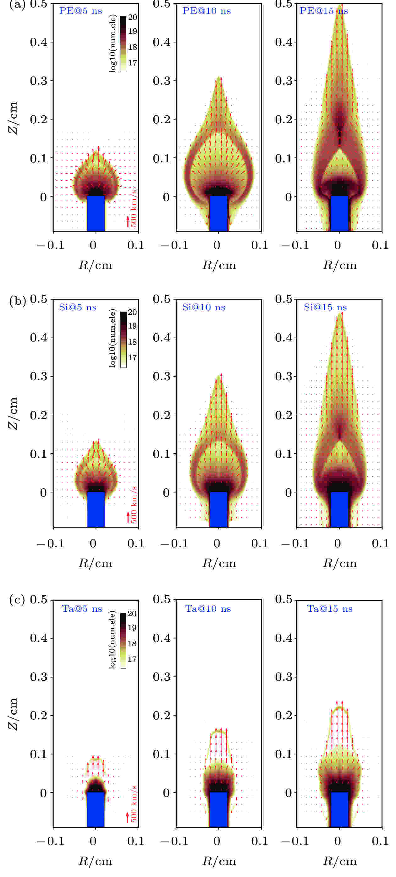
Central outflow’s collimation by magnetic field is an important theoretical mechanism for explaining the astrophysical objects’ morphology formation, and its credibility has been tested in many laser plasma experiments in a dimensionless manner. This article introduces integrated simulation and experiment work based on the present laboratory magnetically collimated jet framework, to explore how non-ideal terms’ strength including radiative cooling and magnetic diffusion from different targets can affect the outflow shape. The interaction between outflow from a target with low atomic number and external field satisfies the ideal magneto-hydrodynamic conditions, and the outflow shape results in diamagnetic cavity and jet; on the other hand, a heavy element target brings strong magnetic diffusion that destroys the collimation structure, together with the stagnation of outflow introduced by radiative cooling, and outflow shape results in weakly collimated hemisphere near the target and a detached magnetized density clump. The detailed dimensionless analysis shows that the large-scale dissipation of jets in young stellar objects can possibly be an analog of the laboratory jet’s magnetic diffusion breakup, also similar structures like the loosely collimated lobes and bright ansaes in planetary nebula can be observed in highly diffusive laboratory outflows. This article shows for the first time that a series of non-relativistic astronomical outflows’ dynamic behaviors can be explained by the non-ideal magneto-hydrodynamic evolution of laboratory plasmas.

2020, 69 (19): 195203.
doi:10.7498/aps.69.20200672
Abstract +
Alternating current rotating gliding arc discharge can produce large-scale, wide-range non-equilibrium plasma at atmospheric pressure. In order to investigate the gliding discharge mode, discharge characteristics and Spectral characteristics of AC rotating gliding arc discharge plasma, high speed camera, oscilloscope and spectrometer are used to collect discharge images and electrical signals of rotating gliding arc synchronously. Thus the dynamic behavior of arc and the characteristics of electric signal in the process of rotating gliding arc can be analyzed. The experimental results show that there are two different discharge modes in the rotating gliding arc discharge process, namely the breakdown gliding discharge mode (B-G mode) and the stable gliding discharge mode (A-G mode). The B-G mode is mainly characterized by high-frequency breakdown phenomenon (breakdown-extinguish-breakdown) during the arc gliding process, while the A-G mode is mainly characterized by stable continuous arc sliding. The paper also discusses the working mechanism in which the working parameters influence the gliding arc discharge characteristics. It is shown that the discharge mode and discharge characteristics of arc are the result of the combined action of excitation voltage and gas flow. When the gas flow is large and the excitation voltage is small, the gliding arc is an unstable discharge dominated by the B-G mode. Conversely, when the excitation voltage is large and the gas flow is small, the gliding arc is a stable gliding discharge dominated by the A-G mode. In addition, in B-G mode, the energy consumption is mainly concentrated in the breakdown moment, and the energy release is mainly pulsed. However, when the gliding arc discharge is in A-G mode, the energy dissipation is mainly used to maintain the continuous existence of the arc without extinguishing, and the energy release is stable and continuous. Affected by the gas flow rate and excitation voltage, the breakdown frequency of the B-G mode is greater than that of the A-G mode. Higher repeat breakdown frequency can cause multiple ionization in the process of gliding arc discharge, which produces more active particles. The research conclusions in this paper provide theoretical support for regulating the operating characteristics of the gliding arc discharge. In engineering application, the discharge mode, breakdown frequency and breakdown current of the gliding arc can be adjusted by changing the working parameters to obtain plasma sources with different characteristics.
CONDENSED MATTER: STRUCTURAL, MECHANICAL, AND THERMAL PROPERTIES
2020, 69 (19): 196101.
doi:10.7498/aps.69.20200665
Abstract +
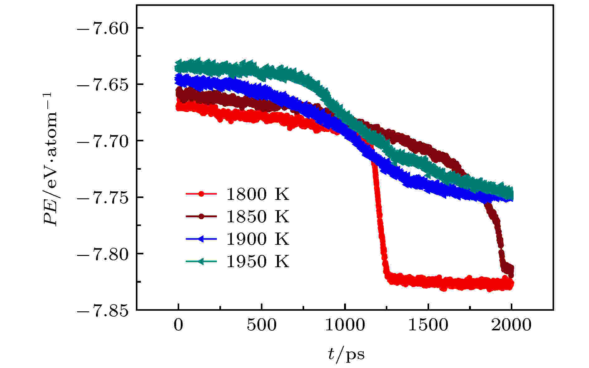
The morphology and physical properties of crystal as well as the glass-forming ability (GFA) of metals are closely related to the evolution pathway of atomic structures in the early stage of nucleation in supercooled liquids. Therefore, the study of the evolution of atomic structures in the isothermal crystallization process of supercooled liquids, is of great significance not only for predicting and accurately controlling the crystal nucleation and growth, but also for understanding the local atomic structural origin of the GFA. In the present work, the atomic-level mechanism for isothermal crystallization in the supercooled liquid tantalum is studied by molecular dynamics (MD) simulation. The microstructural evolution of metal Ta system is characterized and analyzed by using the potential energy per atom (PE), the pair distribution function (PDF) g(r), and the largest standard cluster (LSC). Two crystallization paths of Ta supercooled liquid can be observed during isothermal relaxations. For each pathway the incubation time of the formation critical nucleus increases with annealing temperature (T) rising. At 1800 K ≤T≤ 1850 K, the crystallization of supercooled liquid Ta conforms to the Ostwald's step rule: first, Z12 (i.e. icosahedron) and Z14 (Kasper cluster with 14 coordination number) clusters in supercooled liquids are hinged into medium-range order (i.e., Z-MRO); then the Z-MRO are merged and ordered into A15 crystal phase; finally, BCC crystal nucleus inside of the A15 phase grows rapidly into BCC single crystal at the cost of the atoms in A15 phase. While at 1900 K ≤T≤ 1950 K, Ta supercooled liquid is directly transformed into A15 phase. The A15 crystal phase is mainly formed by the continuous merging of the largest Z-MRO with the small Z-MRO, which is similar to the picture of the classical nucleation theory (CNT). However, whether the phase transition from A15 to BCC will occur above 1900 K remains to be further confirmed by a longer-time MD simulation. Relative to the supercooled liquids of monoatomic metals with lower melting point, the good GFA of Ta may originate from the slowly growing A15 crystal nucleus in its supercooled liquid.
EDITOR'S SUGGESTION
2020, 69 (19): 196102.
doi:10.7498/aps.69.20200836
Abstract +
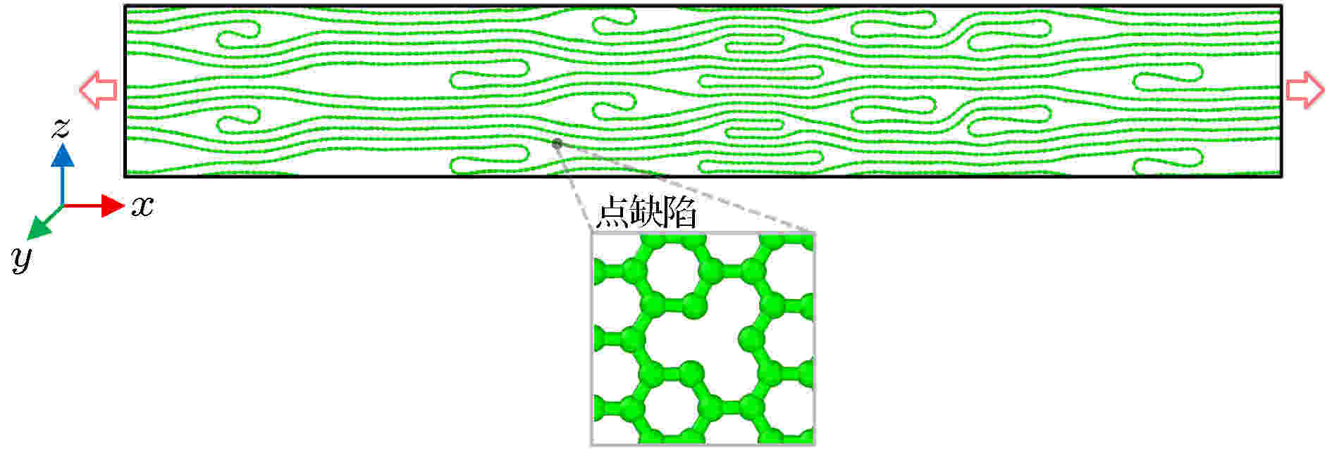
Annealing is a commonly used fabrication technology of graphene-assembled materials, which serves as an efficient method to control material properties. In graphene-assembled materials, the multilayer folded configuration of graphene has been widely observed due to the two dimensional characteristic of graphene. However, the manipulation on the mechanical properties of graphene-assembled materials by annealing has not been fully understood yet, especially considering the effect of folded microstructures. In this paper, we focus on the effect of annealing temperature on the mechanical properties of multilayer folded graphene. The dependences of elastic modulus, tensile strength, ultimate strain and fracture toughness on the annealing temperature have been systematically studied by molecular dynamics simulations. Moreover, the mechanisms behind the manipulations by annealing temperature have been revealed combining the structural evolutions obtained from the simulations. Our results indicate that the multilayer folded graphene after annealing under higher temperature exhibits significant reinforcement on its elastic modulus and tensile strength, while its ultimate strain drops instead. The fracture toughness is enhanced only within a certain range of annealing temperature. The controllable mechanical properties are attributed to the formation of interlayer covalent bonds between carbon atoms belonging to adjacent layers during the annealing processing. With the annealing temperature increases, more interlayer crosslinks are observed from simulations, which greatly strengthens the interlayer interaction. For the cases with lower annealing temperature, the folded graphene can be unfolded easily then finally flattened under tensile stretch, and the structural failure originates from the interlayer slippage in the folded area. However, for the cases with higher annealing temperature, the unfolding deformation is prevented since the folded graphene is blocked by much denser interlayer crosslinks, and the origins of structural failure transforms to the intralayer fracture in graphene plane. Considering the intralayer covalent bond interaction is far more powerful than the interlayer van der Waals interaction, the higher annealing temperature will bring higher elastic modulus and tensile strength due to the change on the structural failure mode, but it will sacrifice the ductility at the same time due to the blocked unfolding process of folded area. It is confirmed in our study that the annealing is an effective approach for the synthetic modulation on the stiffness, strength, ductility and toughness of multilayer folded graphene.
2020, 69 (19): 196601.
doi:10.7498/aps.69.20200737
Abstract +
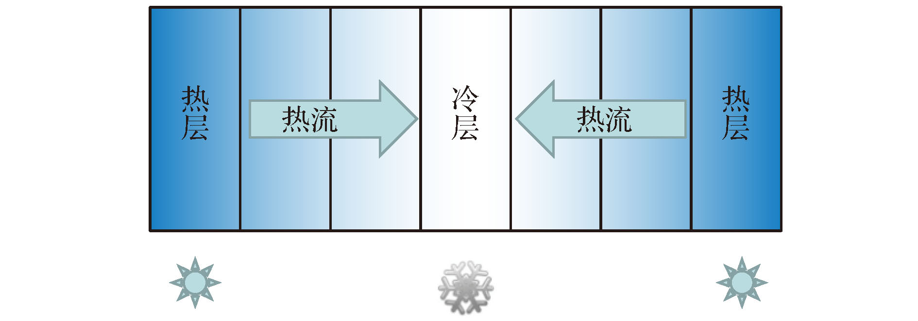
Silicone rubber has an important application as a thermal interface material for its advantages in insulation, heat resistance, etc. The thermal conductivities at different crosslinking densities are calculated by non-equilibrium molecular dynamics. The results show that the thermal conductivity increases with crosslinking density increasing. The thermal conductivity can increase by 40% when the crosslinking density is 80%, which is because the spatial network structure formed by crosslinking shortens the length of heat transfer along the atomic chain, which makes the thermal conductivity increase greatly. The position of crosslinking bond has little effect on the thermal conductivity under the same crosslinking density, i.e. there is no significant difference in the thermal conductivity of the cross-linked structure between the end-cross-linking position and the middle-cross-linking position. However, the increase of the interval between the crosslinking points is beneficial to the increase of the thermal conductivity. The phonon densities of state under different crosslinking densities are calculated, and the heat conduction mechanism of crosslinking structure is analyzed.
2020, 69 (19): 196801.
doi:10.7498/aps.69.20200539
Abstract +
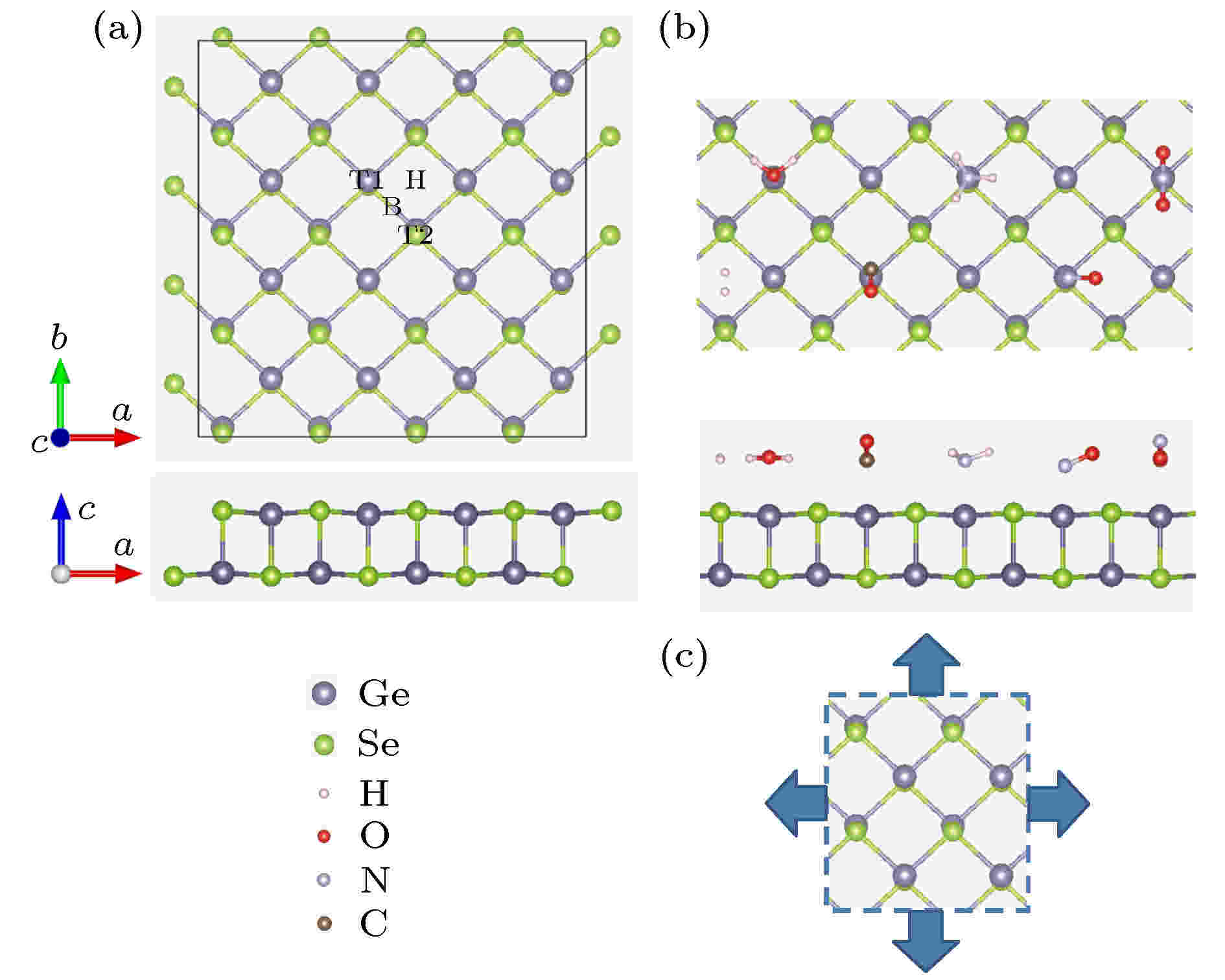
The adsorptions of various gas molecules (H2, H2O, CO, NH3, NO, and NO2) on monolayer GeSe versus the external biaxial strain in a range of –8% to 8% are investigated by first-principles calculations. The band structures, the equilibrium heights, the adsorption energy, and the amount of charge transfer are determined. The calculated results show that monolayer GeSe changes from indirect-to-direct and semiconducting-to-metallic under a certain biaxial strain. The adsorbed gas molecules hardly change the band gap of monolayer GeSe even under a biaxial strain in the whole range from –8% to 8%. The calculated adsorption energies under different strains reveal that the external biaxial strain has no significant effect on the adsorption stability of the gas molecules on monolayer GeSe, so it seems impossible to promote the desorption of the gas molecules by applying strain. It is found that NO2under the biaxial tensile strain of 8% tends to be bound with the monolayer GeSe by chemical bond which leads to being-difficult-to-desorb. Besides that case, the investigated gas molecules are physisorbed on the GeSe surface and have a certain probability of adsorption and desorption. The charge transfers of CO, NH3, NO and NO2adsorbed systems under the biaxial strain from –8% to 8% change somehow but are still non-negligible, while for H2and H2O, their charge transfers are too small to be detected by the monolayer-GeSe-based gas-sensor. Thus, due to the moderate adsorption energy and charge transfer, monolayer GeSe can be a promising candidate as a sensor for CO, NH3and NO under the biaxial strain from –8% to 8%, and for NO2in the range from –8% to 6%. It is worth noting that because of the appropriately lower adsorption energy and bigger charge transfer, a bigger biaxial compressive strain, ranging from –6% to –8%, can improve the response speed and sensibility to CO and NO of monolayer GeSe. Furthermore, the effect of the external biaxial strain on the adsorption stability and the charge transfer are discussed based on the two mechanisms of charge transfers, i.e. the traditional and the orbital mixing charge transfer theory. The charge transfer of NH3is governed by mixing the molecular HOMO with the orbital of GeSe, while for CO, NO and NO2, their charge transfers are most likely determined by different mechanisms under different external strains, which results in different influences on the charge transfer. The present study would be valuable for fully excavating the gas-sensing potential of the two-dimensional GeSe, and then providing sufficient theoretical basis for designing high performance gas sensors based on two-dimensional materials.
CONDENSED MATTER: ELECTRONIC STRUCTURE, ELECTRICAL, MAGNETIC, AND OPTICAL PROPERTIES
2020, 69 (19): 197101.
doi:10.7498/aps.69.20200644
Abstract +
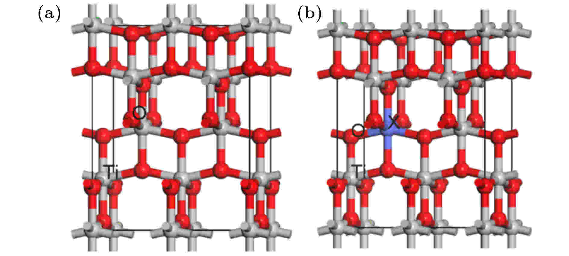
It is still in controversy whether the transition metal doped TiO2will generate room temperature ferromagnetism and where its magnetism originates from. In order to solve this problem, in this paper we use the GGA+U method based on density functional theory to conduct a first-principle study of the magnetic and optical properties for each of the systems of Ti0.875X0.125O2,X= Cr, Mn, Fe, Co. We calculate the ground state energy of each system, on the supposition that they are ferromagnetic or antiferromagnetic. After comparison, the ferromagnetic state is speculated to be its ground state. The binding energy and magnetism calculation results show that Ti0.875Cr0.125O2has the best stability in all doped systems, that the transition metal element doped TiO2system has a net magnetic moment, and that the doped systems are ferrimagnetic. In comparison, the net magnetic moment produced by Cr, Mn and Fe doped with TiO2are substantial, showing that these three systems have good ferromagnetic properties. The Curie temperatures of all doped systems are above room temperature, which is of great significance for the electron spin to retain the information in dilute magnetic semiconductors (DMS), and also greatly helps with the practical application of magnetic materials. The analysis of the energy band structure reveals that intrinsic TiO2is non ferromagnet, Ti0.875Cr0.125O2and Ti0.875Mn0.125O2maintain semiconductor properties, and Ti0.875Fe0.125O2and Ti0.875Co0.125O2exhibit metal characteristics. The doped systems produce room temperature ferromagnetism, the main magnetic source is the transition metal elements (Cr, Mn, Fe, Co) 3d electron orbit induced polarization of the surrounding O-2p state spin electrons, causing the systems to produce a net magnetic moment and be ferromagnetic. The absorption spectrum of the doped system is red-shifted, which shows that the doping causes the range of its absorption spectrum to extend to the visible range. At the same time, in all the doped systems in this article, Fe and Co doped TiO2have the best light absorption intensity, and the magnetic property of the Fe doped system is the strongest, which indicates that when the system is ferromagnetic, the spin up and spin down splitting will occur in the local magnetic field, which will change the electronic structure of TiO2and enhance its photocatalytic performance. The calculation results in this paper are of theoretical significance for preparing TiO2with curie temperature above room temperature bybeing dopedwith transition metal elements of Cr, Mn, Fe, and Co.
2020, 69 (19): 197102.
doi:10.7498/aps.69.20200848
Abstract +
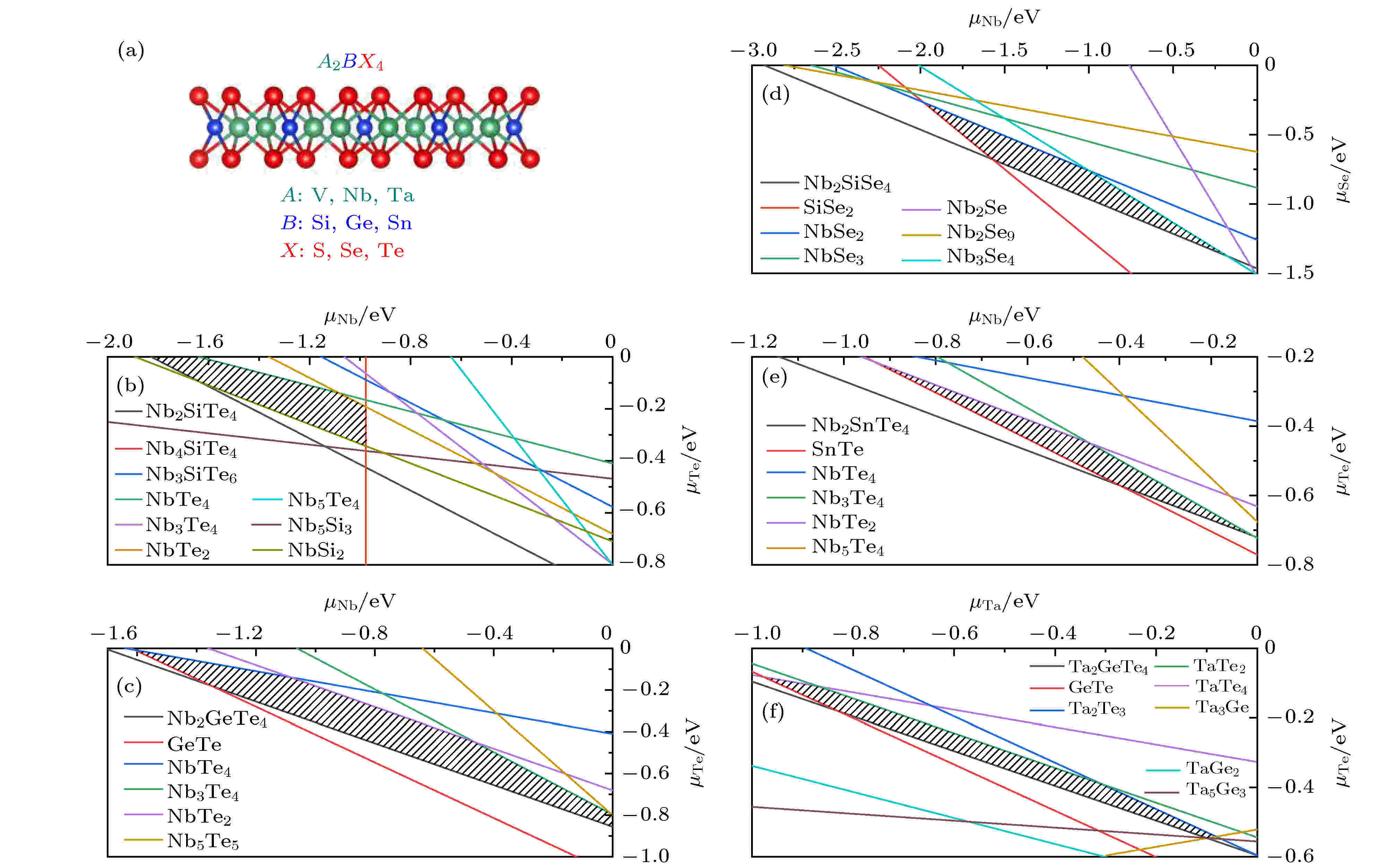
Two-dimensional (2D) niobium silicon telluride (Nb2SiTe4) was recently proposed as a promising candidate in infrared detector, photoelectric conversion, polarized optical sensor and ferroelastic switching application due to its narrow bandgap, long-term air stability, high carrier mobility, etc. However, the in-plane strains and interfacial defects induced by the lattice misfits between functional layers are harmful to 2D heterojunction nanodevice performance, making the crystal-lattice regulation and strain engineering necessary to achieve lattice matching and strain-controllable interface. Here, using first-principles calculations and elemental substitutions, i.e., replacing cations (anions) with elements in the same group of periodic table, we identify three new and stable single-layerA2BX4analogues (Nb2SiSe4, Nb2SnTe4and Ta2GeTe4) as appealing candidates in manipulating the lattice parameters of Nb2SiTe4. The controllable lattice parameters are 6.04 Å ≤a≤ 6.81 Å and 7.74 Å ≤b≤ 8.15 Å. Among them, Ta2GeTe4exhibits similar lattice parameters to Nb2SiTe4but smaller bandgap, yielding better response in far-infrared region. Strain engineering shows that the external biaxial tensile stress narrows the bandgaps ofA2BX4due to the downshifting in energy of conduction band minimum (CBM). External biaxial compressive stress induces valance band maximum (VBM) orbital inversion for Nb2SiTe4, Nb2GeTe4and Ta2GeTe4, which pushes up VBM and discontinues the trend of corresponding bandgap increase. In this case, the bandgap change depends on the competition between energy upshifts of both CBM and VBM. In the Nb2SiSe4and Nb2SnTe4cases, the d-p antibonding coupling in valance band is so strong that no valance band inversion appears while the bandgap increases by ~0.3 eV under −5% compressive strain. Regarding Nb2SiTe4, Nb2GeTe4and Ta2GeTe4, their bandgaps can hardly change under −5% compressive strain, indicating that the energy upshift in VBM equals that in CBM. Such a valance band inversion is attributed to Te outmostporbital overlapping, which introduces more dispersive VBM and smaller effective mass of hole. Our findings suggest that Nb2SiTe4can be alloyed with Nb2SiSe4, Nb2SnTe4and Ta2GeTe4to achieve controllable device lattice matching while maintaining its superior properties at the same time. The use of external biaxial compressive stress can promote the hole diffusion and improve the device performance.
2020, 69 (19): 197301.
doi:10.7498/aps.69.20200104
Abstract +
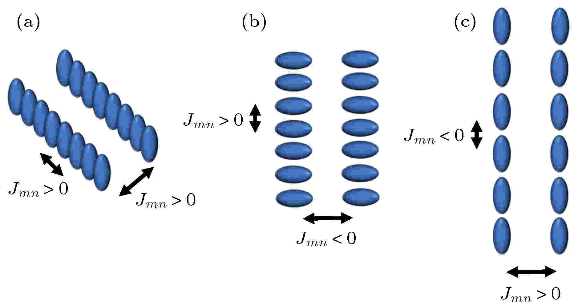
Details of exciton dynamics in dye aggregates and supra-molecular complexes are substantially important for the functionality of molecular based opto-electronic devices. There are intensive theoretical studies of the multi-exciton dynamics in quantum dot structures but much less in molecular systems. Multiple excitons can be produced in molecular chains as well as two-dimensional and three-dimensional aggregates under an excitation of ultrafast strong laser pulse. According to the dipole arrangements of molecular chains, the coupled molecular chains are designed as H-H, H-J and J-H types of dipole configurations. In the scheme of density matrix theory, the dynamic processes of multiple excitons of different configurations are investigated by solving the quantum master equation through using the approximate dipole-dipole and expectation values of interest. The equations of motion for expectation values of interest governing the respective density operator are used to describe the temporal evolution of the multi-exciton states. It is found that the exciton energy band can be formed in the energy representation, and the multiple excitons are delocalized in the aggregates. The excitons represent different temporal evolutions excited by different resonant excitations. Compared with single-chain systems, double-chain systems have different degrees of blue shift or red shift due to interchain coupling. In the H-H type of aggregate, the electron population is lower if the double-molecule chain is simultaneously excited by the resonance frequency of a single molecule; the electron population increases to a certain extent if the frequency of the field is higher than the vibration frequency of a single molecule. The band width and the energy levels of the multiple excitons vary for different configurations of coupled molecular chains, and the wave packets show their own characters in these energetic levels. In the H-H type of aggregate, exciton state has priority to occupy the high-order energy level. The width of the exciton band of H-J type is significantly narrower than that of H single or H-H double chain configuration, because the Coulomb interaction of the inter-stranded dipole moment makes the whole energy low. In the J-H aggregates, the exciton states are more stable from the energy point of view, and the exciton energy band is wide because of the large Coulomb interaction. The energy of exciton state can be transferred via the interchain coupling, no matter which chain is excited. The transfer period directly correlates with the nearest interchain coupling.
2020, 69 (19): 197701.
doi:10.7498/aps.69.20200655
Abstract +
2020, 69 (19): 197801.
doi:10.7498/aps.69.20200580
Abstract +
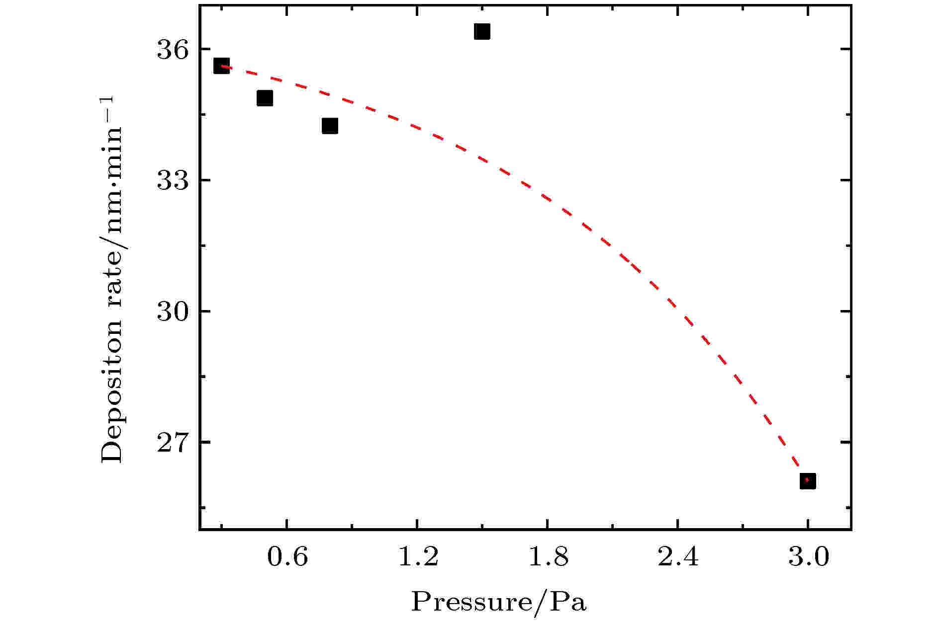
Transparent conductive oxide (TCO) films, as transparent electrodes, are widely used in thin-film solar cells. The performance of TCO film has a significant influence on the conversion efficiency of the film solar cell fabricated byusing it. Although the conductivity can be improved by increasing the carrier concentration, the transmittance in the long wave will be sacrificed. Therefore, the only feasible method is to increase the carrier mobility within a certain carrier concentration range, rather than increase the mobility by reducing carrier concentration. In this paper, the F and Al co-doped ZnO (FAZO) films are deposited on glass substrates (Corning XG) by an RF magnetron sputtering technique with using a small amount of ZnF2(1 wt.%) and Al2O3(1 wt.%) dopant. The influences of sputtering pressure on the structure, morphology and photoelectric characteristics of the films are respectively investigated by X-ray diffraction analysis, scanning electron microscope, Hall effect measurement, and ultraviolet–visible–near infrared spectrophotometry. All the thin films show typical wurtzite structure with thecaxis preferentially oriented perpendicular to the substrate. With the increase of sputtering pressure, the deposition rate of FAZO film decreases, the crystallization quality is deteriorated, surface topography changes gradually from “crater-like” to co-existent “crater-like” and “granular-like”, and the surface roughness increases. The FAZO film deposited at 0.5 Pa presents the optimal performance with a mobility of 40.03 cm2/V·s, carrier concentration of 3.92 × 1020cm–3, resistivity of 3.98 × 10⁻⁴Ω·cm, and about 90% average transmittance in a range of 380-1200 nm. The theoretical result shows that the co-doping of F and Al takes the advantages of single F and Al doped ZnO films, and overcomes the shortcoming of metal elements doping, which donates the carriers just from doped metal elements. Furthermore, the co-doping of F and Al not only increases the carriers but also reduces the scatterings caused by the inter-orbital interaction of doped atoms. The doped F 2p electron orbitals repel the O 2p and Zn 4s electron orbitals, making them move down and donate electrons. At the same time, the orbitals of Al 3s and Al 3p also make a contribution to the conductivity. After co-doping of F and Al, both the carrier concentration and conductivity increase significantly.
INTERDISCIPLINARY PHYSICS AND RELATED AREAS OF SCIENCE AND TECHNOLOGY
2020, 69 (19): 198101.
doi:10.7498/aps.69.20200641
Abstract +
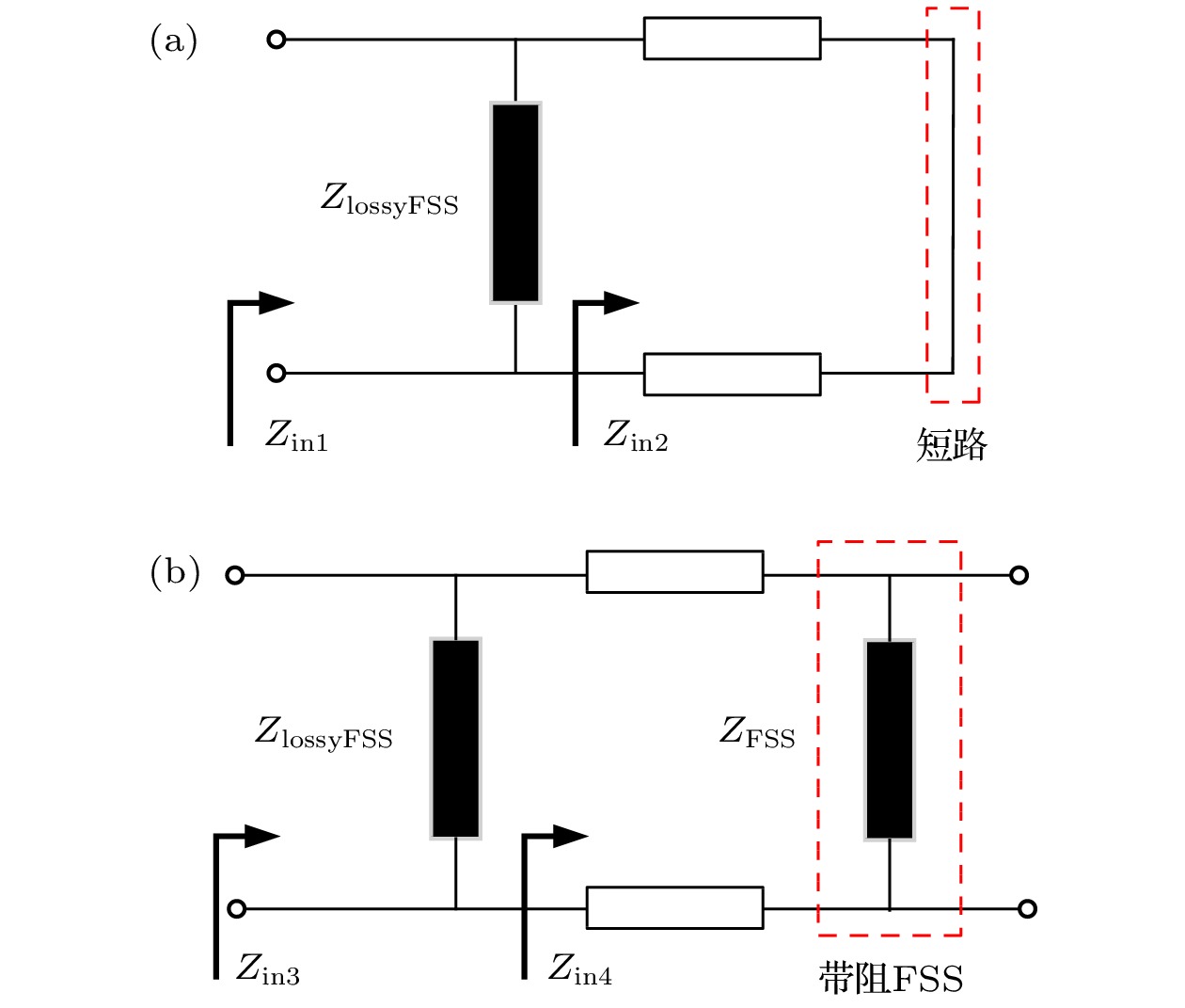
In this paper, a single polarized absorptive frequency selective surface (AFSS) with ultra-wide transmission band and broad absorption band has been proposed numerically and experimentally. Based on the principle of circuit analog absorber (CAA), the proposed wideband AFSS is realized via replacing the ground plane with a band-stop frequency selective sturcture. The proposed AFSS is finally a hybrid structure composed of a wideband lossy frequency selective surface (FSS) in the top and a 3D band-stop frequency selective structure in the bottom. The wideband lossy FSS with thinner profile in the top is realized by utilizing a low pass capasitive elements to compensate the equivalent load inductance arising from the air space that is less than quarter wavelength installing between FSS and ground plane, and the low pass capactive lossy FSS is synthesized using “Gong”-shaped patterns with lumped resistors. Meanwhile, the unit cell of 3D frequency selective structure consists of two electrical coupling C-shaped patterns is investigated to achieve a wide stop band with high selectivity, which can be equivalent to the ground plane in the absorption band. By cascading the wideband lossy FSS and the 3D band-stop frequency selective structure, a thinner hybrid AFSS is presented with ultra-wide transmission band and broad absorption band. The results obtained from simulation shown that an absorption band with absorptivity above 90% is obtained from 6.6 to 11.6 GHz, and the 1 dB transmisson band is from 1 to 3.5 GHz with minimum insertion loss of 0.21 dB. Moreover, the performance can be guaranteed for TE-polarized oblique incidence up to 30°. Finally, a prototype is fabricated to validate its performance, the measured results shown that the 1 dB transmission band ranges from 1 to 3.5 GHz, and the absorption band is operating from 6.3 to 11 GHz at normal TE-polarized incidence. A good agreement between the experiment and simulation results is achieved, which verifies the effectiveness of the design.

2020, 69 (19): 198102.
doi:10.7498/aps.69.20200701
Abstract +
Despite the fact that three-dimensional organic-inorganic hybrid perovskite is regarded as a promising material in the field of optoelectronics and microelectronics due to its excellent photoelectric properties, however, the instability under the moisture environment and the gate-voltage screening effect associated with ionic transport are still serious, which restricts the development of perovskite devices. Here in this work, the lead iodide perovskite (PEA)2(MA)n–1PbnI3n+1series are successfully prepared by one-step solution method, including pure-two-dimensional (pure-2D), quasi-two-dimensional (quasi-2D) and traditional three-dimensional (3D) perovskite materials. The dimension and microstructure of the perovskites are regulated, and the effects of dimensions on the performance of organic-inorganic hybrid perovskite materials are investigated firstly. The crystallization of the 2D perovskites and 3D perovskite films are observed obviously. Moreover, the surface of pure-2D perovskite film with discoid, regular and micron-sized grains is smoother than that of 3D perovskite film. And also, the unapparent grain boundary is exhibited in the quasi-2D perovskites. A uniform perovskite film with full coverage and inconspicuous grain boundaries facilitates the transmission capacity of the charge carriers in the channel layer due to the reduction of defects caused by the grain boundaries. And benefited from the high-quality films with inconspicuous grain boundary as demonstrated, the quasi-2D hybrid perovskite film exhibits a longer carrier lifetime (τns) than traditional 3D MAPbI3perovskite film, revealing that the layered 2D structure is more favorable for carrier transport due to the fewer defects in it. In addition, under the condition of the same environment humidity, the 2D perovskite materials show better moisture stability. Then, to investigate the influences of dimensional structure on the perovskite field-effect devices, we fabricate the bottom-gate and top-contact thin film transistors (TFTs) based on the perovskite materials with different dimensions. As a result, the instability and ion migration effect for each of the devices are suppressed effectively due to the distinct 2D layer-structure and quantum confinement effect, which leads the device performance to be further improved. The device based on quasi-2D (n= 6) channel TFT achieves a hole mobility (μhole) of 3.9 cm2/(V·s), an on-off current ratio of 104and more, and a 1.85V turn-on voltage of 1.85 V. The first application of quasi-2D organic and inorganic hybrid perovskite materials to thin film transistors provides a new idea for preparing the high-performance and stable thin film transistor devices.
EDITOR'S SUGGESTION
2020, 69 (19): 198201.
doi:10.7498/aps.69.20200230
Abstract +
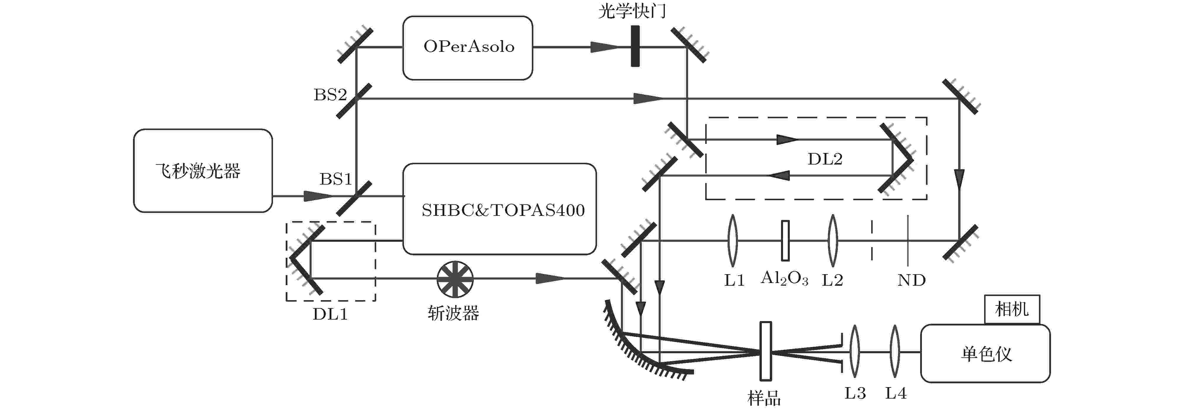
As one of the most fundamental processes, proton transfer reaction plays an important role in chemical and biological process, and to reveal the choreography of the proton motion intra- and intermolecularly, a spectroscopic technique capable of capturing molecular structural dynamics of excited-state proton transfer motions on an intrinsic time scale is needed. In this study, We utilize wavelength-tunable femtosecond stimulated Raman spectroscopy with a time resolution of ~100 fs, spectral resolution of 15 cm–1and spectral range of 400 cm–1—1800 cm–1, combined with traditional transient absorption spectroscopywith a time window between 0 and 600 ps to simultaneously achieve reaction dynamics for transient reactant and product of the photoacid pyranine (8-hydroxypyrene1, 3, 6-trisulfonic acid, HPTS) molecules undergoing excited-state proton transfer reaction in complex with water and acetate molecules. Marker bands attributed to the deprotonated form of HPTS in a frequency range from 400 cm–1to 1700 cm–1are obtained under the excitation of 400 nm laser pulses. The marker band at 1516 cm–1, which is assigned to phenolic ring carbon carbon double band stretching accompanied with carbon hydrogen in-plane rocking motions, exhibits complex rise and decay dynamics. The simultaneously observed excited-state Raman mode at 920 cm–1which is assigned to the excited carbon-carbon single bond stretch mode in the protonated acetic acid root molecule, helps us to clearly resolve the reaction rates of excited-state proton transfer. Based on the multi-exponential fitting results, the dynamics of excited-state Raman mode at 920 cm–1exhibits bi-exponential processes with time constants of ~470 fs and ~3 ps. The ultrafast time component indicates that the excited-state proton transfer originates from an HPTS-acetate complex, indicating that part of the ground-state HPTS molecules are in the “tight” hydrogen bonding configuration that can quickly shift the excited-state proton charge toward the acetate acceptor molecule through a direct hydrogen bond. The second slower time component implies a significant subpopulation of HPTS in the ground state, i.e. hydrogen bonds to an acetate ion via an intervening water molecule, and upon photo excitation, the proton transfers to the water solvent before proton is picked up by the acetate ion.
2020, 69 (19): 198401.
doi:10.7498/aps.69.20200383
Abstract +
2020, 69 (19): 198502.
doi:10.7498/aps.69.20200228
Abstract +
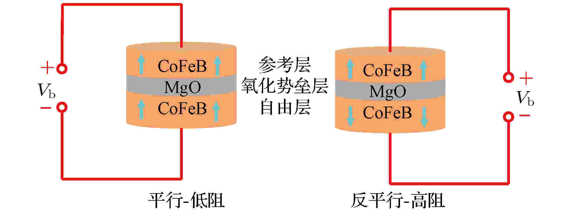
As one of the primary elements in magnetoresistive random access memory (MRAM), voltage controlled magnetic anisotropy magnetic tunnel junction (VCMA-MTJ) has received wide attention due to its fast read and write speed, low power dissipation, and compatibility with standard CMOS technology. However, with the downscaling of VCMA-MTJ and the increasing of storage density of MRAM, the effect of process deviation on the characteristics of MTJ becomes more and more obvious, which even leads to Read/Write (R/W) error in VCMA-MTJ circuits. Taking into account the depth deviation of the free layer (γtf) and the depth deviation of the oxide barrier layer (γtox) in magnetron sputtering technique as well as the etching process stability factor (α) caused by the sidewall re-deposition layer in the ion beam etching process, the electrical model of VCMA-MTJ with process deviation is presented in the paper. It is shown that the VCMA-MTJ cannot achieve the effective reversal of the magnetization direction whenγtf≥ 13% andγtox≥ 11%. The precession of magnetization direction in VCMA-MTJ also becomes instable whenα≤ 0.7. Furthermore, the electrical model of VCMA-MTJ with process deviation is also applied to the R/W circuit to study the effect of process deviation on the R/W error in the circuit. Considering the fact that all ofγtf,γtox, and α follow Gauss distribution, The 3σ/μis adopted to represent the process deviation, with using Monte Carlo simulation, whereσis the standard deviation, andμis the average value. It is shown that the write error of the circuit goes up to 30 % with 3σ/μof 0.05 and the voltage (Vb) of 1.15 V. At the same time, the read error of the circuit is 20% with 3σ/μof 0.05 and driving voltage (Vdd) of 0.6 V. Both the read error rate and the write error rate of the VCMA-MTJ circuit increase as process deviation increases. It is found that the write error rate can be effectively reduced by increasingVband reducing the voltage pulse width (tpw). The increasing ofVddis helpful in reducing the read error rate effectively. Our research presents a useful guideline for designing and analyzing the VCMA-MTJ and VCMA-MTJ read/write circuits.

2020, 69 (19): 198701.
doi:10.7498/aps.69.20200674
Abstract +
Compared with traditional X-ray imaging systems based on polycapillary X-ray optics or a pinhole, coded aperture imaging system has the advantages in simple structure, high sensitivity, and strong expandability, which make it possess the potential applications in X-ray fluorescence imaging. In this work, a new coded aperture X-ray imaging system based on a novel imaging model which decomposes the mask projections into a superposition of two separable functions is designed and proposed for high-resolution X-ray imaging. The performance of the system is demonstrated by using the Geant4 package. To reduce the computational complexity of calibration and image reconstruction, a separable mask with 90 × 90 pixels is used. The mask is designed by selecting the central part of the original rank 463 modified uniformly redundant arrays. The mask is made of platinum foil with a pixel pitch of 25 microns. To study the effect of mask thickness on system performance, the mask thickness is varied from 25 to 200 microns. The active area of the Si detector employed in the system is 2 mm × 2 mm, divided into 80 × 80 pixels, each with a size of 25 μm × 25 μm. The field of view of the system is equal to the area of the detector, which is 2 mm × 2 mm. The detector is parallel to and center-aligned with the mask with a fixed distance of 2.0 mm. The images are reconstructed by using the fast iterative shrinkage-thresholding algorithm. The high-quality reconstructed images of different energy line sources and complex shaped objects are obtained. The simulation and analysis results indicate that for the near-field imaging, unlike imaging systems based on the conventional convolution model, the system has the performance that is not affected by the aperture collimation effect. The spatial resolution of the imaging system is about 65 microns. The calibrated matrices used have an important influence on the image quality. The quality of the reconstructed image is affected by the energy of X-rays used during calibration and the energy of X-rays emitted from the object; the smaller the difference between these two energy values, the higher the quality of the reconstructed images will be. The three-dimensional reconstruction results show that the system can correctly estimate the distance between the object and the system from a single two-dimensional projection. The axial spatial resolution of the system is about 1.1 mm.
2020, 69 (19): 198801.
doi:10.7498/aps.69.20200624
Abstract +
REVIEW
COVER ARTICLE
2020, 69 (19): 198501.
doi:10.7498/aps.69.20200742
Abstract +
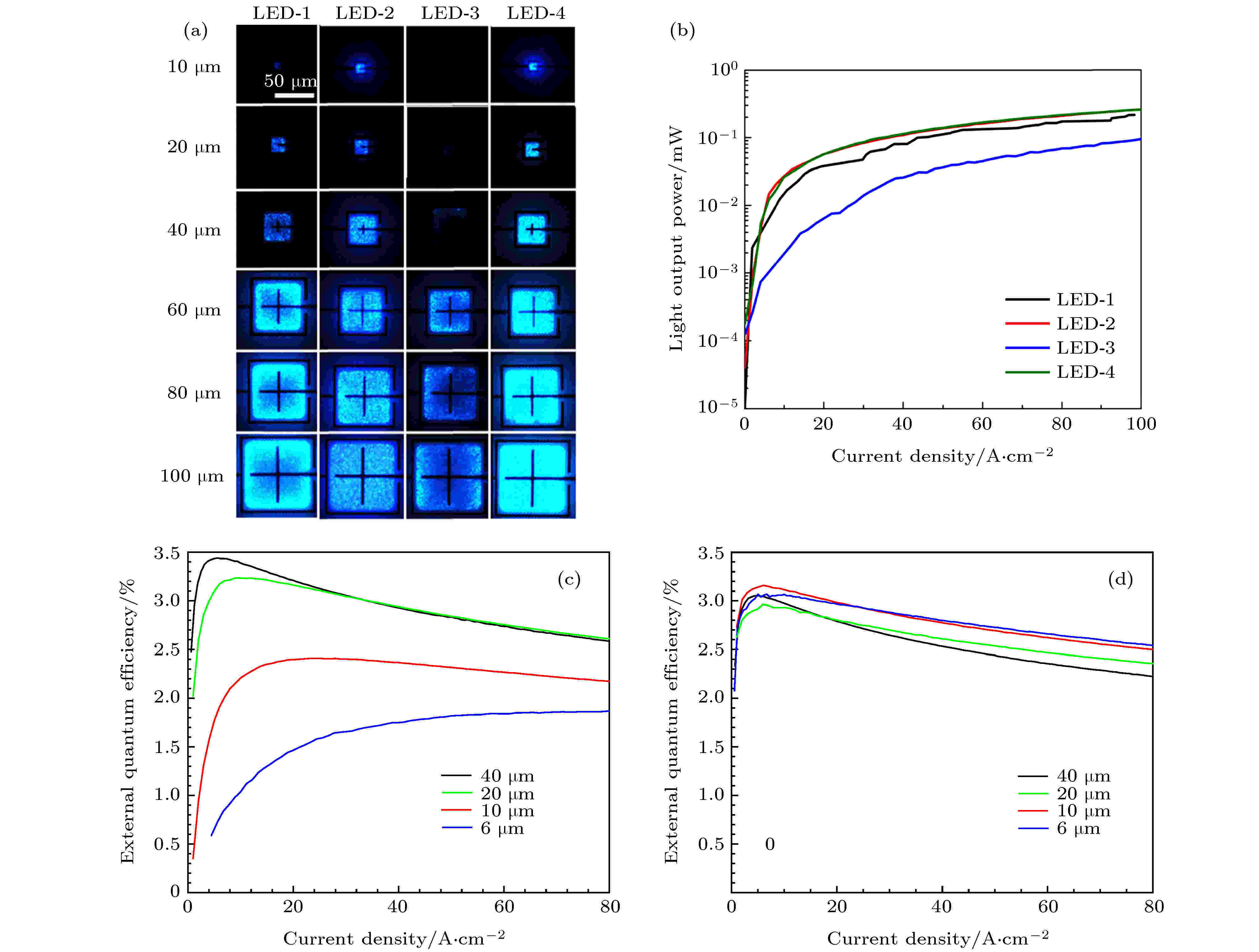
The continuous miniaturization and integration of pixelated devices have become a main trend in the field of display. Micro light-emitting diode (micro-LED) display is composed of an array of LEDs that are sub-50-micrometers in length. It has huge advantages in brightness, resolution, contrast, power consumption, lifetime, response speed and reliability compared with liquid crystal display (LCD) and organic LED (OLED) display. Consequently, micro-LED display is regarded as the next-generation display technology with high potential applications, such as virtual reality (VR), augmented reality (AR), mobile phones, tablet computers, high-definition TVs and wearable devices. Currently, the combination of commercial 5G communication technology with VR/AR display, ultra high definition video technologies will further prompt the development of micro-LED display industry. However, some basic scientific and technological problems in micro-LED display remain to be resolved. As the chip size shrinks to below 50 μm, some problems that are not serious for large-sized LEDs appear for micro-LEDs. These problems include crystalline defects, wavelength uniformity, full-color emmision, massively tranferring and testing, etc. In the past two decades, various solutions to those problems have been proposed, which have greatly promoted the progress of micro-LED display. In this paper, an overview of micro-LED display since 2000 is given firstly, which includes the main research results and application achievements. Secondly the issues involved in the wafer epitaxy and chip process of micro-LEDs and possible solutions are discussed based on the display application in detail. The surface state induced by the dangling bonds and dry etching damages are concerned for the nonradiative recombination at a low injection level. The remedies are provided for those surface states, such as atomic-layer deposition and neutral beam etching. Some methods to reduce the threading dislocation and suppress the polarization field are summarized for micro-LED epitaxial growth. Moreover, the GaN-based LEDs on Si (100) substrate are also introduced for the future integration of micro-LEDs into the Si-based integrated circuits. As to the wavelength uniformity, the MOCVD equipment and growth technology including the laser treatment are discussed. In the chip processing part, the full-color display, mass transfer and effective inspection technology are discussed. Assembling RGB individual LEDs, quantum dot phosphor material and nanocoloumn LEDs are different routes for full-color display. Their trends in the future are provided. The pick and place, laser lift-off technologies, are strengthened in the massively transferring for micro-LEDs. In the massively and rapidly inspection technologies, the photoluminscence combined with Raman scattering, the electroluminescence combined with digital camera are discussed. Finally, the summary and outlook in these issues are also provided.


