SPECIAL TOPIC—Perovskite optoelectronic devices and physics
2019, 68 (15): 158506.
doi:10.7498/aps.68.20190675
Abstract +
When there is a strong spin-orbit coupling in some direct semiconductor with an inversion-asymmetric structure, the Rashba effect will exist, splitting the spin-degenerated bands into two sub-bands with opposite spin states. These two sub-bands will deviate from the symmetry center of the Brillouin zone, making the semiconductor an indirect band gap semiconductor. Metal halide perovskites exhibit strong spin-orbit coupling and possess an inversion-asymmetric crystal structure, showing great potential in Rashba effect research. In this review, we systematically review the Rashba effects in perovskites, including the theoretical and experimental studies for demonstrating the Rashba effect in perovskites, the influence of Rashba effect on the carrier recombination, and the current debates concerning the Rashba effect in perovskites. Then, several problems that need to be solved urgently are proposed,they being 1) whether there exists the Rashba effect in the perovskite, 2) whether the Rashba effect can exert a significant influence on carrier recombination, and 3) what the relationship between the Rashba effect and the perovskite stucture is. The prospects are also given for the future research including the study of the Rashba effect in perovskites by various spectral methods and the applications of the Rashba effect in optical-electronic-magnetic devices.
EDITOR'S SUGGESTION
2019, 68 (15): 157101.
doi:10.7498/aps.68.20190596
Abstract +
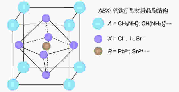
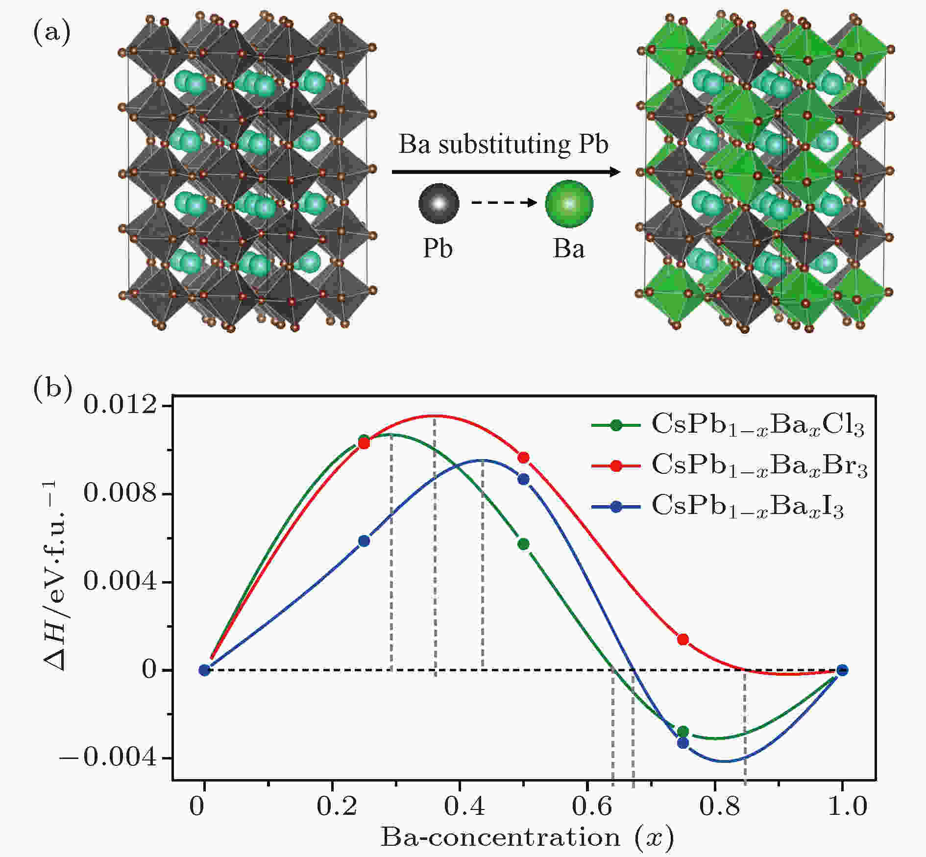
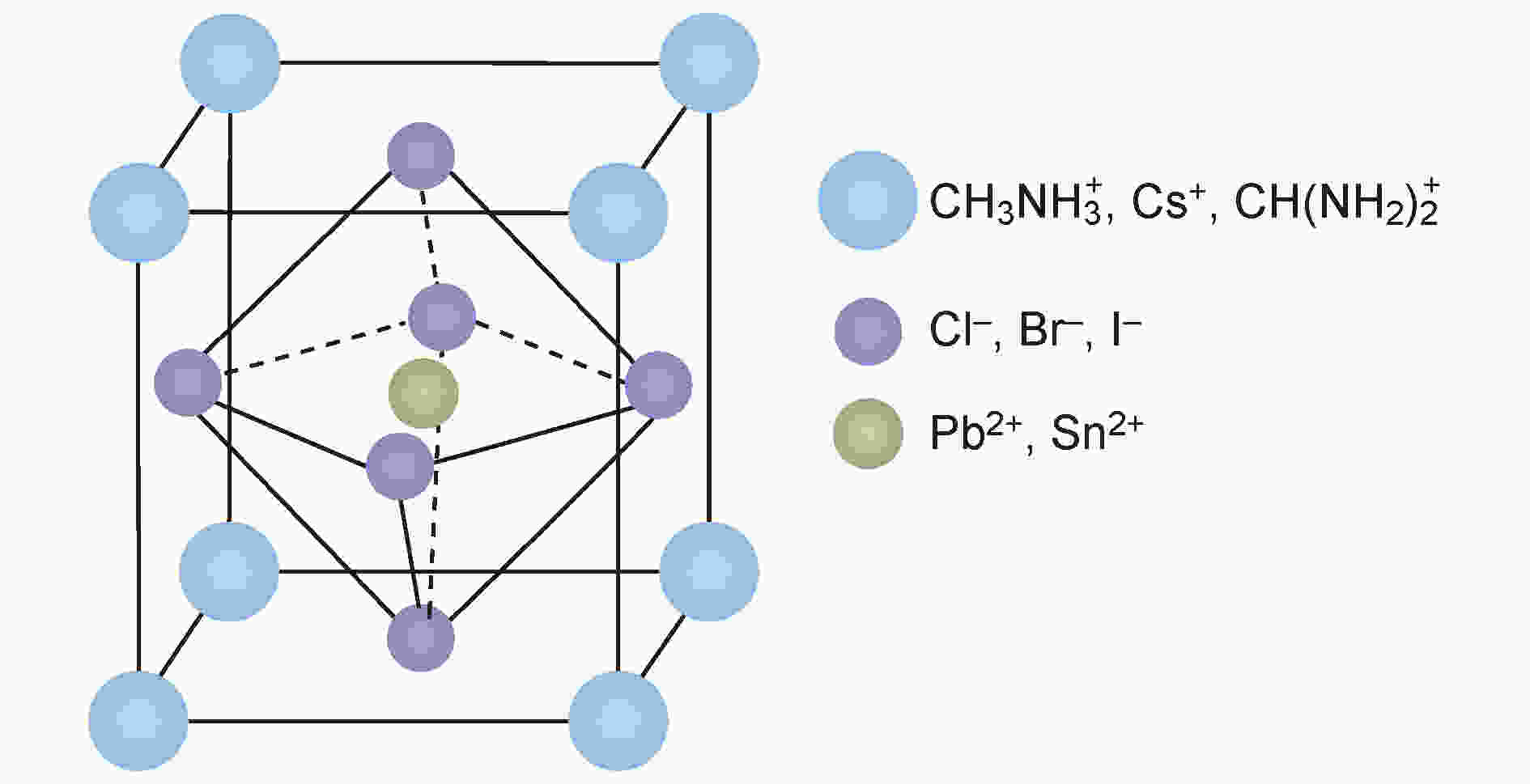
Organic-inorganic halide perovskitesABX3(A= CH3NH3, HC(NH2)2;B= Pb;X= Cl, Br, I) have recently attracted increasing attention due to their advanced optoelectronic properties. However, the poor stability and toxicity of organic lead halogen perovskites are still a major challenge for deploying the outdoor solar cells. Element substitution is a simple and effective strategy to solve these problems. For example, the substitution of the I ions with Cl and Br has been regarded as a reliable method to improve the device stability.A-site engineering, i.e., replacing organic ions with inorganic cations (such as Cs+, Rb+), has also been reported. TheB-site alloying approach has been demonstrated with Zn, Sr, Sn, etc. Inorganic halide perovskites can be synthesized by the low-cost solution spin-coating method and have similar optoelectronic properties and improved stability to their organic counterparts. Here in this paper, we report a comprehensive study of the alloyed perovskite CsPb1–xBaxX3(X= Cl, Br, I) by combining the disorder alloy structure search method with first-principles energy calculations. We find that it is not easy to dope barium into the perovskite lattice when Ba concentration is low and the stable disordered solid solution can exist in the high Ba concentration case. Carrier effective mass and bandgap increase with the increase of Ba concentration and the bandgap change range is wide, owing to the difference in both electronegativity and ionic radius between Pb and Ba. After inducing Ba into CsPb1–xBaxX3(X= Cl, Br, I), the higher electron concentration on the I sites also enhances the Coulomb interaction of the Pb—I bonds. Moreover, the electrons and holes tend to be located on Pb sites, and this may give rise to the formation of local potential wells, which would further induce the large lattice deformation to accommodate the self-trapped excitons. Especially, CsPbI3-Pnmaperovskite is metastable in the ambient environment with a suitable photon absorption threshold. The CsPb1–xBaxI3can be used as a capping layer on CsPbI3in solar cells, thereby significantly improving the power conversion efficiency and long-term stability. Overall, the alloyed perovskite CsPb1–xBaxX3(X= Cl, Br, I) with high Ba concentration can be stable and less-toxic, and they can be used in short wave light-emitting diodes, radiation detectors or other fields because of their large bandgaps (> 2.8 eV).
2019, 68 (15): 157102.
doi:10.7498/aps.68.20190324
Abstract +
Lead halide perovskites, which can be grown by solution process, are very suitable for various optoelectronic applications, such as in solar cells, light-emitting diodes, lasers and photo-detectors, due to their outstanding electrical and optical properties. However, lead halide perovskites are unstable under continuous light illumination, which severely degrades the performance and lifetime of optoelectronic devices based on them. Therefore, the photo-stability of perovskites and the mechanisms have received more and more attention. In this article we review the main phenomena in perovskites, induced by continuous light illumination, namely photo curing, photo dissociation, photo-induced phase separation, and photo-induced phase transition. The proposed mechanisms for the instability from the perspectives of defect states, ion migration, thermodynamics and chemical bonds, respectively, are also introduced. Finally, the complexity presented in the studying of photo-stability, and the issues should be addressed in the future are also briefly discussed.
2019, 68 (15): 158401.
doi:10.7498/aps.68.20190569
Abstract +
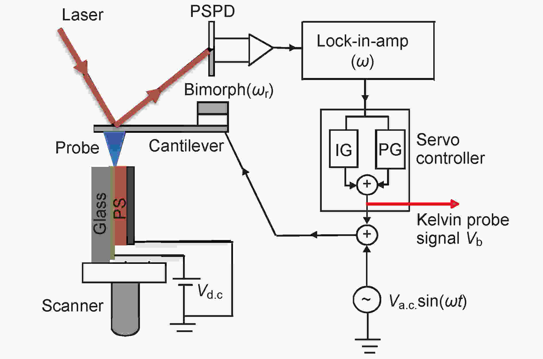
Perovskite solar cells, as a promising next-generation photovoltaic technology for large-scale application, have demonstrated the advantages of high absorption coefficient, tunable bandgap, considerable photoelectric conversion efficiency and low-cost fabrication. However, the photoelectric conversion process within the device is still not understood clearly. One of the major reasons is that it is difficult to directly observe the space potential inside the device and its effect on the photogenerated charge carriers. The direct measurement and analysis of the space potential inside the device and the clarification of the intrinsic relationship between the space potential and the charge carrier micro-process under illumination and different electric field conditions can reveal the photoelectric conversion mechanism in depth, and thus providing the scientific research basis for the further development. Kelvin probe force microscopy (KPFM), a testing technology that is non-contact, can detect the space potential distribution without any damage to the device, demonstrating the great potential to unveil the working mechanism of perovskite solar cells accurately. Such a characterization method can work under vacuum condition. The KPFM combines Kelvin method of measuring contact potential difference with the scan probe microscopy to characterize internal carrier dynamic behavior with high resolution on a nanometer scale. The study of the spatial potential distribution of semiconductor device plays an important role in understanding the working mechanism of new perovskite solar cells. For example, under an open-circuit condition, the intensity and width of the electric field and space charge region can be obtained from the spatial potential distribution, and the bending direction of the energy band can be judged according to the increase or decrease of the potential. While in a short-circuit case, the generation and transport of charge carriers can be obtained. In this review, we mainly introduce the research progress of the space potential distribution and optoelectronic conversion mechanism in perovskite solar cells. The key mechanism of charge carrier generation, separation, transport and recombination are revealed by using KPFM to directly observe the space potential variations caused by light or electric field. We also prospect the issues and challenges in the future research.
2019, 68 (15): 158503.
doi:10.7498/aps.68.20190745
Abstract +
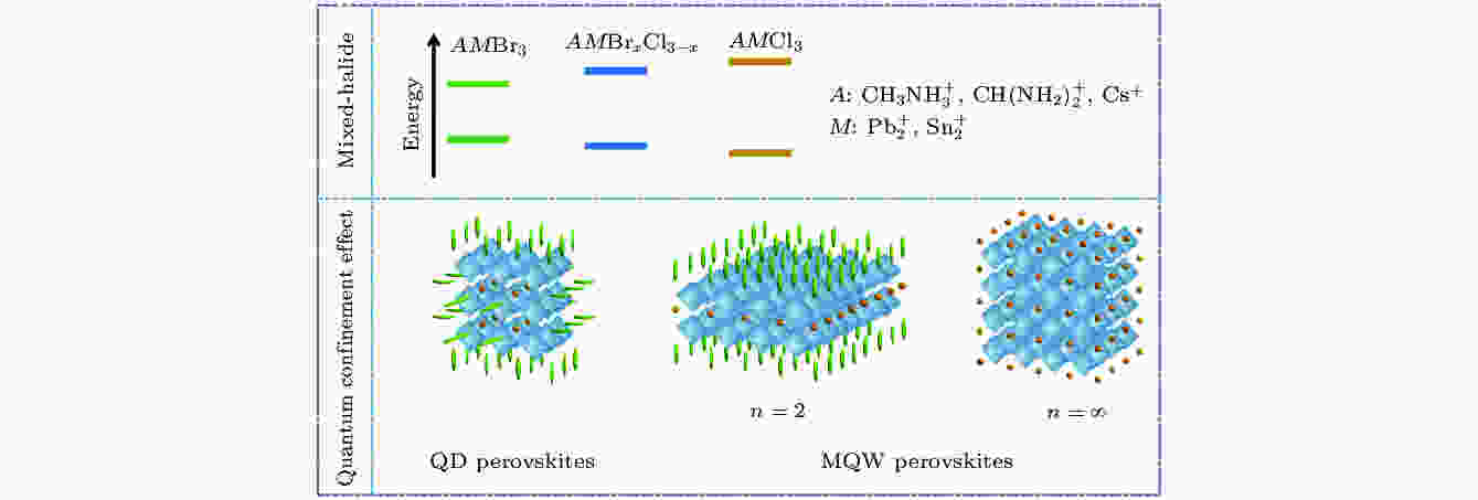
The great progress of light-emitting diodes (LEDs) has been made based on perovskites, and the external quantum efficiency of near infrared, red and green devices have reached > 20%, exhibiting their great potential applications in lighting and displays. However, the performance of blue perovskite LEDs is very poor, thus limiting their applications in the field of full-color displays. The blue perovskite LEDs can be achieved through mixed halides or quantum confinement effect. In this paper, we review the research progress of blue perovskite LEDs based on these two strategies, discuss the challenges to achieve high-performance perovskite LEDs and present our perspectives.
2019, 68 (15): 158504.
doi:10.7498/aps.68.20190647
Abstract +
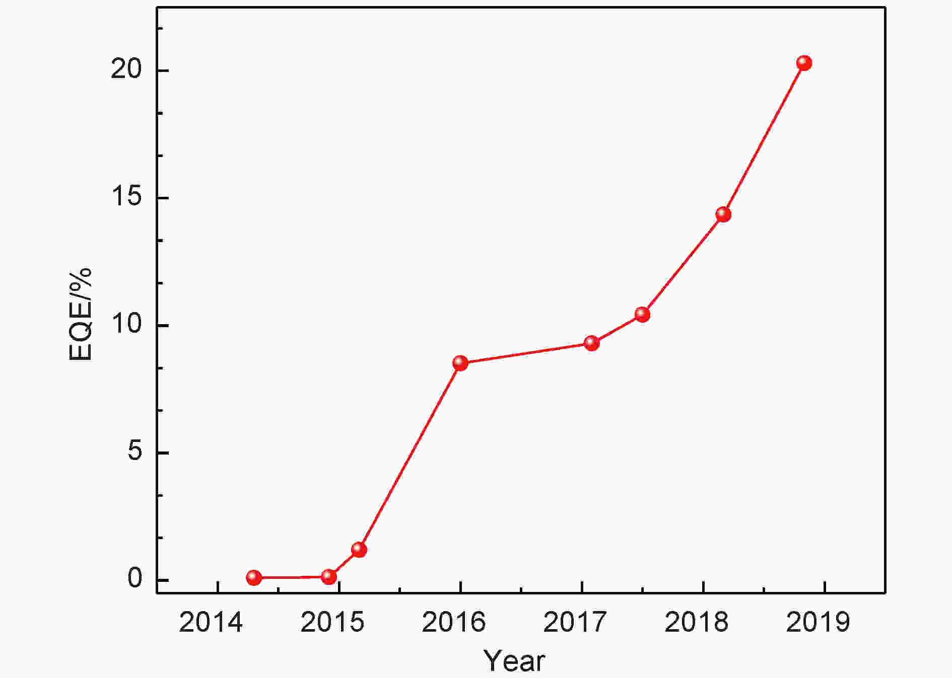
Perovskite light emitting diodes exhibit the advantages of high color purity, tunable wavelength and low producing cost. Considering these superiorities, one regards perovskite light emitting diodes as very promising candidates for solid state lighting and panel displaying. Human eyes are very sensitive to green light, thus green perovskite light emitting diodes receive the most attention from researchers. Since the advent of the very first green perovskite light emitting diode, the external quantum efficiency has climbed from only 0.1% to over 20%. In this review, we mainly discuss the history of green perovskite light emitting diodes, the basic concepts of perovskite materials and green perovskite light emitting diodes, and the common methods to improve the efficiency of green perovskite light emitting diodes. The bandgap of bromide perovskite is about 2.3 eV, which is located just on a green light wavelength scale and thus becomes the suitable emitting layer material for green emission. There are mainly two types of device structures, i.e. regular format and inverted format. The whole working process of green perovskite light emitting diodes can be divided into two stages, i.e. the injection and recombination of charge carriers. One engineers the energy levels of different layers to improve the injection of charge carriers. They also raise up the strategy so-called surface passivation to reduce the defect density at the interface in order to avoid the quenching phenomenon. One usually inserts a buffering layer to realize the surface passivation. Besides, perovskites possess very small exciton binding energy, which is at the same order of magnitudes as the kinetic energy at room temperature. Charge carriers become free in this case, which will severely reduce the radiation recombination probability due to the non-radiation recombination process such as Shockley-Read-Hall effect and Auger recombination. To solve the problem, people fabricate three types of perovskites, namely quasi two-dimensional perovskite, perovskite quantum dot, and perovskite nanocrystal. In this way, the charge carriers can be confined into a limited space and the exciton binding energy will hence be improved. From the efficiency perspective, the green perovskite light emitting diodes promise to be commercialized. However, another critical issue impeding the development of green perovskite light emitting diodes is the stability problem. Comparing with the organic light emitting diodes and inorganic quantum dot light emitting diodes, the lifetime of perovskite light emitting diodes is too limited, which is only approximately one hundred hours under normal conditions. The temperature, moisture and light exposure are all factors that influence the stability of perovskite light emitting diodes.
2019, 68 (15): 158505.
doi:10.7498/aps.68.20190307
Abstract +
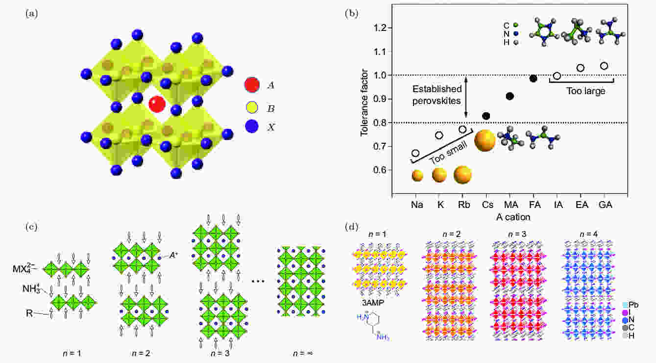
In recent years, metal halide perovskites have received extensive attention due to their superior optoelectronic properties and solution processability, which also become a research hotspot in the field of optoelectronics. Among all the perovskite optoelectronics applications, perovskite light-emitting diode (LED) becomes one of the important research topics because it is likely to be used in the next-generation display technique. Based on the high photoluminescence quantum yield (PLQY), facilely tunable bandgaps, and sharp emission of perovskite material, the external quantum efficiency of perovskite LED has increased from less than 1% to over 20% within only five years, showing the most rapid development speed in the LED field. During the 5-year exploration of perovskite LEDs, researchers have focused their efforts on how to realize the crystal-growth control in the perovskite film formation process, enhance PLQY of the perovskite films, and improve the performance of perovskite LEDs. Among all the approaches, the utilization of organic additives including small molecules and polymers proves to be an effective strategy. Here, in this article, we review the recent advances in metal halide perovskite LEDs based on the strategy of organic-additive treatment. We also analyze and discuss the interaction between organic additive and perovskite crystal as well as its influence on the performance of perovskite LED. In the end, we discuss the challenges remaining in perovskite LEDs and the prospects for perovskite LEDs.

2019, 68 (15): 158801.
doi:10.7498/aps.68.20190853
Abstract +
In recent years, metal halide perovskite solar cells have attracted widespread attention due to their unique technological superiority. Remarkable progress of device performance has been achieved in last few years. The certified efficiency has reached 24.2%, which is close to the efficiency of the commercial crystalline silicon solar cells. Halide perovskite is a kind of semiconductor and ionic conductor material, which not only has the ability to transfer charges, but also exhibits the phenomenon of ion migration under an external electric field. Ion migration can directly change the local chemical ratio of perovskite crystals, and can also greatly affect the electrical properties of materials and the working mechanisms of corresponding devices. In this review, the formation mechanism, basic characteristics and effects of ion migration on the working mechanism of the device (such as giant switchable photovoltaic phenomenon, current hysteresis, etc.) are summarized, and then some recent advances in the suppression of ion migration are introduced. Since there exist still many doubts about ion migration in perovskite materials, it is very important to understand the phenomenon of ion migration in perovskite materials in order to promote the development and application of perovskite solar cells.
2019, 68 (15): 158802.
doi:10.7498/aps.68.20190306
Abstract +
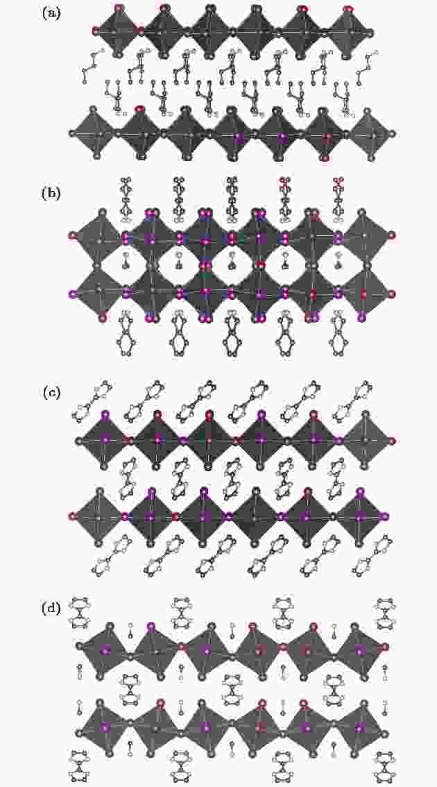
Hybrid perovskites are a series of solution-processable materials for photovoltaic devices. To achieve better performance and stability, interface passivation is an effective method. So far, the most commonly used passivators are organic amines, which can tailor perovskite into a lower-dimensional structure (Ruddlesden-Popper perovskite). Here, we select a biimizole (BIM) molecule as a new passivator for perovskite. The BIM based single layer perovskite has a more rigid structure. And multi-layered structure cannot be formed due to large lattice mismatching and structural rigidity. By inducing the excess MAI (methanaminium iodide) into the lattice, the layered structure is maintained, and half of the BIM molecules are replaced by MA (methylamine). The mixed layered structure is distorted, because of the difference in size between two kinds of cations. We then investigate passivation effect of BIM on perovskite solar cells. By carefully controlling the feed ratio in precursor solutions, we fabricate solar cells with different passivation structures. We find that the introduction of BIM can causeVocto increase generally, indicating that MAPbI3is well passivated. The peak at 7.5° and 15° in X-ray diffraction pattern are corresponding to a two-dimensional (2D) phase with a shorter layer distance. There are no peaks at lower degrees, so that no multi-layered structure is formed in the film either. We suppose that a dual-phase 2D-3D (where 3D represents three-dimensional) structure is formed in the perovskite film. To explain the passivation effect of the two 2D structures, we investigate their lattice matching towards MAPbI3. The distorted 2D structure is well matched with (110) face of o-MAPbI3, and the mismatching rate is lower 1% in the two directions. On the other hand, the BIM based 2D structure cannot well match with (–110) face of o-MAPbI3, nor with (001) face of c-MAPbI3. We also consider that the less rigidity of distorted structure contributes to better passivation. As a result, we achieve a BIM passivated perovskite solar cell with a power conversion efficiency up to 14%. This work paves a new way to the interface engineering of perovskite solar cells.
2019, 68 (15): 158803.
doi:10.7498/aps.68.20190468
Abstract +
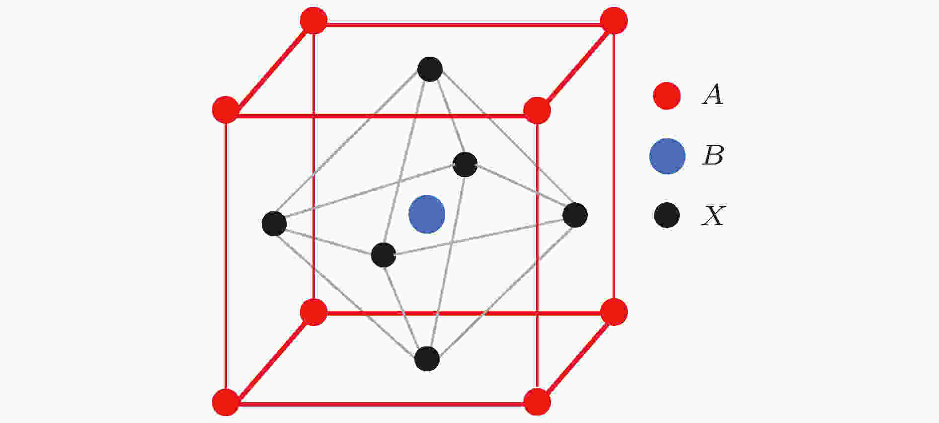
In recent years, organic-inorganic hybrid perovskite solar cells have aroused the interest of a large number of researchers due to the advantages of large optical absorption coefficient, tunable bandgap and easy fabrication. Recently, the power conversion efficiency of organic-inorganic hybrid perovskite solar cells has been enhanced to more than 23% in laboratory. In solution processed perovskite solar cells, perovskite and charge transport layer are stacked together, due to the different crystallization rates leading to lattice mismatch near the surface region of perovskite film, resulting in a lot of interface defects, especially at the interface between perovskite and charge transport layer. What is more, the photo-induced free carriers must transfer across the interfaces to be collected. But the defects near the interface can trap photogeneration electrons, thus reducing the carrier lifetime and causing the charges to be recombined, which greatly influence the performance and stability of perovskite solar cells. Therefore, reducing and passivating these defects is critical for obtaining the high performance perovskite solar cells. Now, there have been made tremendous efforts devoting to advancing passivation techniques, such as doping and surface modification, for high efficiency perovskite solar cell with improved stability and reduced hysteresis. These approaches also contribute to improving the energy band alignment between carrier transport layers and perovskite absorber improving device performance, or resistance moisture to enhance device stability. In this review we mainly introduce the formation and the effect of defects on perovskite solar cells, analyze the mechanism for passivating the interfacial defects between charge transport layer and perovskite photo absorption layer for different materials, compare the effects of different passivation materials on the photovoltaic performance of perovskite solar cells, and summarize the role of these materials in passivating the defects. Finally we discuss the research trend and development direction of passivation defects in perovskite solar cells.
2019, 68 (15): 158804.
doi:10.7498/aps.68.20190343
Abstract +
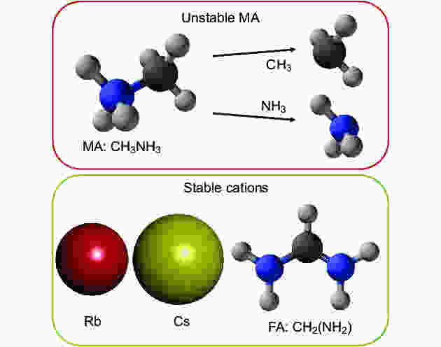
The power conversion efficiency of organic-inorganic hybrid perovskite solar cell has exceeded 24%. The rapid increase in efficiency coupled with its cost-effective fabrication has attracted tremendous attention toward the commercialization of perovskite solar cells. The biggest challenge that hinders the commercialization of perovskite solar cells is the long-term instability of materials and the corresponding devices, which cannot compete with other commercialized solar cells, such as Si cells, in terms of lifetime. The intrinsic instability of perovskite material itself is the most critical challenge faced by researchers. In this study, we discuss the intrinsic instability of organic-inorganic hybrid perovskite materials from the aspects of both chemical instability and phase instability. Suggestions for improving the stability of perovskite solar cell are provided from the perspective of composition design and fabrication process.
2019, 68 (15): 158805.
doi:10.7498/aps.68.20190303
Abstract +
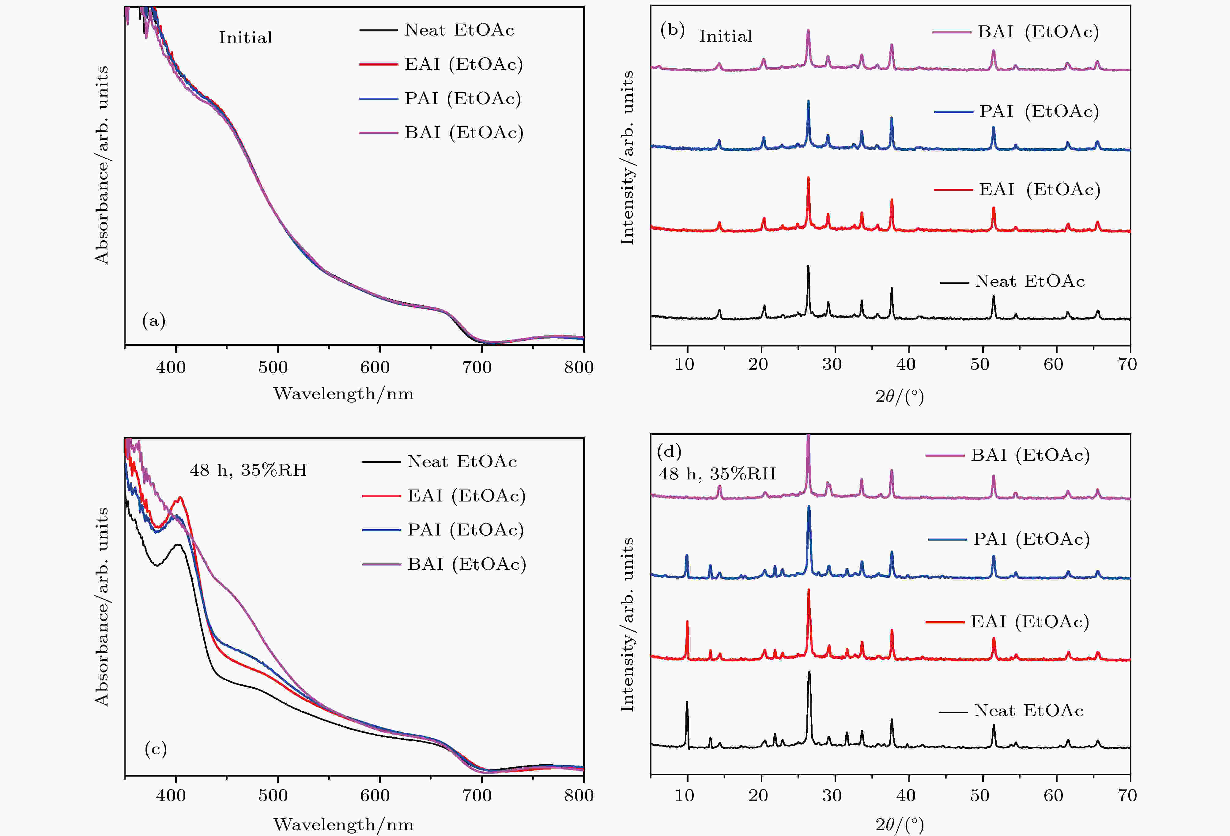
All-inorganic perovskite cesium lead halides with superior stability, suitable bandgap and high absorption efficient have become a promising candidate for photovoltaic application. In all-inorganic cesium lead halide perovskites, CsPbX3(X= Br, I) exhibits excellent photoelectric properties, which are similar to those of organic-inorganic hybrid perovskites. The CsPbI3faces a challenge of unideal tolerant factor for perovskite phase while CsPbI3–xBrxhas better tolerant factor. Among them, CsPbI2Br is one of most popular candidates because of its good thermal stability. Nevertheless, CsPbI2Br shows instability due to the phase transition caused by moisture and lower efficiency because of defects. For all inorganic perovskite devices, the alkyl chain length of surface treatment agent should be taken into account when using organic cationic passivation method. In this paper, CsPbI2Br perovskite is treated with different organic ammonium salts to enhance its phase stability. The experimental results show thatα-phase CsPbI2Br is more stable with the increase of the alkyl chain length. Butylamine iodine (BAI) among three kinds of surface treating agents is proved to have the best defect passivation and phase stabilization effect. With the increase of alkyl chain length, the hydrophobicity of the organic molecular layer increases, which plays a crucial role in protecting optically active CsPbI2Br. Meanwhile, it is found that the stability of perovskite is enhanced with the concentration of the BAI solution increasing. This should be related to the organic cation termination formed on the surface of CsPbI2Br film. Solar cell devices based on the CsPbI2Br thin films treated with different concentrations of BAI are assembled and then the effect of organic ion surface treatment on the photoelectric performance of batteries is further explored. The experimental results show that when the concentration of BAI is relatively high (4 mg/mL and 8 mg/mL), the device’s photovoltaic performance decreases especially the photocurrent obviously decreases, while the post-treatment process using 2 mg/mL BAI will enhance not only the phase stability but also the photovoltaic parameters after defect passivation. Considering both humidity resistance and device efficiency, this work demonstrates that the CsPbI2Br thin film with suitable BAI treatment can improve the wet stability of perovskite, and enhance the photovoltaic performance.
2019, 68 (15): 158806.
doi:10.7498/aps.68.20190355
Abstract +
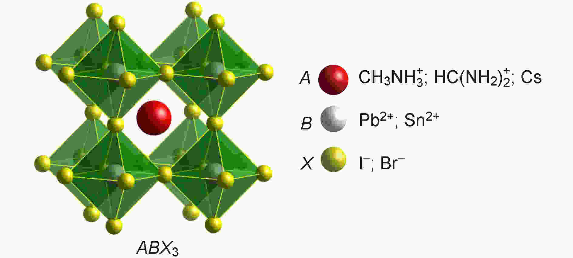
Photovoltaic technology, which can converse solar illumination into electricity, is crucial to the sustainable development of human civilization. Among them, the organic-inorganic hybrid perovskite solar cell (OIPSC) has become a research front due to its excellent photoelectric characteristics, low production cost and high power conversion efficiency (PCE). Although the PCE of OIPSC has exceeded 24%, the organic components in the perovskite system are sensitive to the decomposion caused by either being exposed to light or heated in high temperature environment. The stability defects have greatly limited the commercialization of perovskite solar cells. Therefore, it is urgent to improve the stability of perovskite solar cells, especially to solve the material decomposition problem. All-inorganic perovskite photovoltaic material, composed of all-inorganic elements, exhibits excellent heat and moisture resistance. Therefore, the development of all-inorganic perovskite solar cells is of great significance for solving the current stability problems in perovskite photovoltaics. In this work, we review the recent research progress of all-inorganic perovskite solar cells, discuss the solution approaches to processing all-inorganic perovskite films, and explore the enhancement of device stability. Our work provides a guideline for further promoting the device stability and PCE.

2019, 68 (15): 158807.
doi:10.7498/aps.68.20190302
Abstract +
In the field of photovoltaic materials, perovskite has attracted extensive attention during the past years, owing to its excellent photovoltaic properties, including high charge carrier mobility, low exciton binding energy, long charge carrier diffusion length, broad light absorption spectrum, large absorption coefficient, and low-cost solution processability. However, due to the limitations of film preparation methods (typical spin coating), industrial large-scale production of perovskite solar cells is still in infancy. The inkjet printing technology is a significant manufacturing technology developed from home and office printing and widely used in various printing electronics industries. Compared with other deposition methods, it possesses many advantages, including low cost, high material utilization, high patterning precision, etc. As a direct writing technology, the inkjet printing has shown great industrial potential and is expected to be employed in the industrialization of perovskite solar cells. In this paper, we review the research progress of perovskite solar cells fabricated via the inkjet printing and the application of inkjet printing technology to various functional layers (electrode, hole transport layer, electron transport layer, perovskite active layer). Finally, the challenges of inkjet printed perovskite solar cells at this stage are discussed, and the commercialization direction of inkjet printed perovskite solar cells is also pointed out.
GENERAL
INVITED REVIEW
2019, 68 (15): 150301.
doi:10.7498/aps.68.20190385
Abstract +
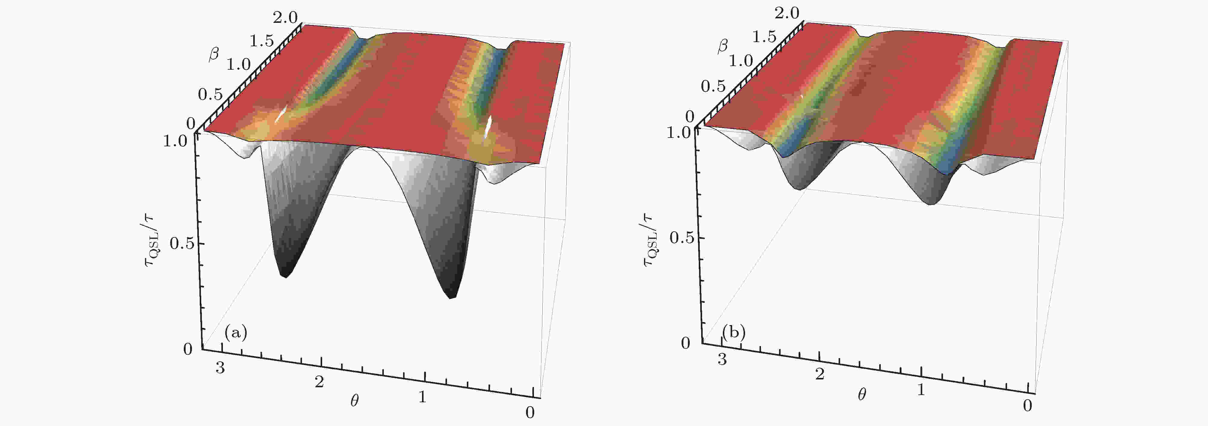
We consider a two-mode entangled coherent light field, in which one mode of the light field is injected into the cavity and interacts with a two-level atom. According to the theory of cavity electrodynamics, the evolution state of atomic system is deduced. Aiming at the dynamic process from the initial state of an atomic system to the target evolution state, the quantum speed limit time is used to characterize the maximum evolution rate of the quantum state of an atomic system. The maximum evolution rate of an atomic system can be controlled by adjusting the coherent parameters of the two-mode entangled coherent light field. But up to now, which kind of quantum speed limit time can be better, universal and strict applicable to the quantum dynamics process of any system is still an unresolved important issue. Based on different methods of measuring the distance between two quantum states and different dynamic evolution channels, many definitions of the quantum speed limit time have been given. The quantum speed limit time proposed by Deffner and Lutz (Deffner S, Lutz E 2013Phys. Rev. Lett.111010402) and the other deduced by Campaioli et al. (Campaioli F, Pollock F A, Binder F C, Modi K 2018Phys. Rev. Lett.120060409; Campaioli F, Pollock F A, Modi K 2018 arXiv:1806.08742) have attracted extensive attention. In this paper, we first compare the advantages of two quantum speed limit times to characterize the maximum evolution rate of quantum states. We find that the quantum speed limit time expression given by Campaioli et al. (Campaioli F, Pollock F A, Modi K 2018 arXiv:1806.08742) in 2018 is a tighter bound when describing the boundary of the shortest time required for the quantum state evolution of a two-level atomic system. Therefore, this paper is mainly based on the quantum speed limit time given by Campaioli et al. to analyze how to achieve the maximum evolution rate of the quantum state of the atomic system by manipulating the parameters of a two-level entangled coherent light field. The results show that the maximum evolution speed of the quantum state of the atomic system can be significantly affected by the coherent parameters of the light field interacting with the atom under certain conditions. Furthermore, when the interacting light field parameters cannot well control the maximum evolution speed of the quantum state, the quantum correlation with the two-mode entangled coherent light field can realize the remote control of the maximum evolution speed of quantum state of atomic system by the light field parameters that are not involved in the atom-light interaction.
2019, 68 (15): 150501.
doi:10.7498/aps.68.20190191
Abstract +
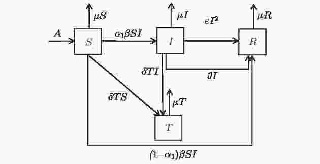
In the process of rumor propagation, people who know the truth or judge the truth can spread true information about rumors. Therefore, on the rumor propagation, it is significant to introduce the spreaders who spread true information in the rumor propagation. But the previous studies did not take into consideration the influence of true information spreading on the rumor propagation. In this paper, the susceptible-infective-true-removed (SITR) rumor propagation model with the true information spreader and the forgetting factor of rumors is established. The thresholdK0is obtained by using the method of the next generation matrix. IfK0< 1, the balance between no rumor and no true information spreader is locally asymptotically stable. The existence and stability of two boundary balance (that is, there are rumor spreaders but no true information spreaders, and there are no rumor spreaders but true information spreaders) are proved. The bistable region of two-boundary balance is given. Further, under different conditions we obtain the existence and locally asymptotical stability of positive balance (rumor spreaders and true information spreaders coexist). Finally, the theoretical results are verified by numerical simulations. We find that the initial value of the true information spreaders affects the peak value of the rumor spreaders and the duration of the rumor. The bigger the initial value of the true information spreaders, the smaller the peak value of the rumor spreaders is and the shorter the duration of the rumor is. The initial value of the rumor spreaders affects the peak value of the rumor spreaders, and the time when the rumor spreaders reach the peak value. The larger the initial value of the rumor spreaders, the larger the peak value of the rumor spreaders is and the earlier the peak value appears. But the initial value of the rumor spreaders does not affect the duration of the rumor. Therefore, in the process of rumor propagation, according to mathematical analysis of the rumor propagation model, we find that the rumor spread is a very complicated process. The results of mathematical analysis can provide theoretical basis to control the rumor propagation and reduce the negative effects of rumors.
NUCLEAR PHYSICS

COVER ARTICLE
2019, 68 (15): 152501.
doi:10.7498/aps.68.20181717
Abstract +
Fission reaction rate is an important index for validating and checking the neutron transportation and fission power in nuclear engineering. The experimental data can be used in benchmark validation of cross sections, and in studying the correlation of fission power with the thickness of uranium sphere shell. There are five assemblies of depleted uranium shells used in this work, the inner radii of which are all fixed at 13.1 cm, while their outer radii are 18.1, 19.4, 23.35, 25.4 and 28.5 cm, respectively. The D-T neutron source is generated in the center of the assemblies, the yield of which is about 3 × 10¹⁰−4 × 10¹⁰s–1. In horizontal plane across the center of the assemblies, the fission rates at positions along the radial direction are measured in the direction with 45° inclining with respect to the incident D+beam. Due to the disturbance to assemblies and neutron field, the activation foil of uranium is a suitable choice rather than fission chamber or capture detector. The material of activation foil is the same as that in the experimental assemblies. Considering the accurate fission yield of143Ce, the objective nuclides are selected. The total fission yield of143Ce is contributed by238U and a little235U. For calculating the total fission yiled of143Ce, the neutron energy range of 0−15 MeV is divided into eight subranges. By measuring the 293 keV gamma rays from the fission product143Ce in activation foils with a TRANS-SPEC-DX100 HPGe detector, with a relative efficiency 40%, the fission rates and the trends at positions along the radial direction in the five assemblies are obtained based on the143Ce fission product yield. The fission rate ranges from 5.28 × 10⁻²⁹to 7.58 × 10⁻²⁸sn-1·nuclide–1, with the relative uncertainty in a range from 6% to 11%. The Monte Carlo transport code MCNP5 and continuous energy cross section library ENDF/BV.8 are used for analyzing the fission rate distribution in the assemblies, and the experiemtal configuration, including the wall of the experimental hall is described in detail in the model. The calculated results are compared with the experimental ones and their agreement is found to be in an uncertainty range.
ELECTROMAGNETISM, OPTICS, ACOUSTICS, HEAT TRANSFER, CLASSICAL MECHANICS, AND FLUID DYNAMICS
2019, 68 (15): 154101.
doi:10.7498/aps.68.20190283
Abstract +
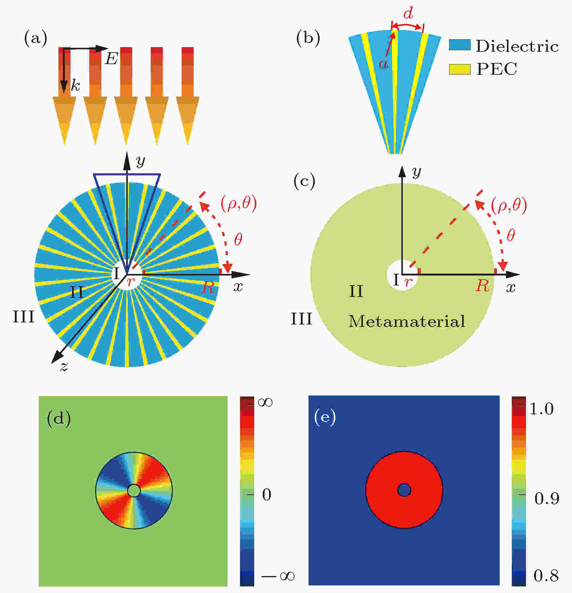
Surface plasmons include surface plasmon polaritons and localized surface plasmons, which are electromagnetic wave confined at the interface of the metal and dielectric. Spoof surface plasmonic structure has many special optical properties, which is of great significance for designing new-generation optical elements. In order to transfer the features of the surface plasmon polaritons and localized surface plasmons to microwave-terahertz region, Pendry et al. (Pendry J B, Martin-Moreno L, Garcia-Vidal F J 2004Science305847) have proposed the spoof surface plasmon polaritons based on a metal structure with grooved stripes. In this paper, a hollow textured perfect electric conductor cylinder with periodic cut-through slits structure is designed to suppress the light scattering of the object in any direction and achieve the effect of omnidirectional cloaking while the transverse magnetic polarization wave propagates along thexdirection. And the locations of the electrical and magnetic modes can be freely modulated by tailoring the structural geometric construction. In order to find the physical mechanism behind the abnormal phenomenon, through theoretical analysis and numerical simulation, we find that the strong scattering suppression of this spoof surface plasmonic polariton structure is caused by the interference between the background wave and Mie scattering of the structural unit, and it can be equivalent to a ring metamaterial due to the special structural design, in order to achieve the omnidirectional cloaking. It implies that we can hide objects in metal strips due to the fact that the metal in the microwave-to-terahertz region is equivalent to a perfect electrical conductor. This opens up a new way to analyzing the physical cloaking and optical response of spoof surface plasmonic polaritons structure. In addition, we also analyze the influence of the structure on the movement law of the scattering spectrum under different structural parameters. This enables us to have an in-depth understanding of the influence of structural parameters on the structural scattering spectrum. Our results can be applied to the microwave-to-terahertz region and a variety of advanced optic devices such as radars, cloaking coatings, sensors and detectors.

2019, 68 (15): 154102.
doi:10.7498/aps.68.20190264
Abstract +
Extended interaction klystron is a very important millimeter-wave and sub-millimeter-wave vacuum electron device with many actual and potential applications, such as space-borne cloud profiling radar, communication, imaging system, precision guided missiles, etc. Kinematical theory and space charge wave theory are extensively used to analyze the bunching process of electrons. Kinematical theory is precise when electron beam is especially small because the influence of space charge effect is ignored, while space charge wave theory is accurate when the modulation of electron beam is small since it is based on the premise of small amplitude. Based on kinematical theory, law of induce current, principle of charge conservation in a one-dimensioanl mode and small signal condition, the influence of electron beam on standing wave electric field in multiple-gap cavity is analyzed, and the expression of beam-loading conductance and beam-loading susceptance in multiple-gap cavity are derived. The influence of the direct current transmit angle of single gap, the number of multiple gaps and the direct current transmit angle of between center of adjacent gaps on beam-loading conductance and beam-loading susceptance are analyzed. The results show that the beam-loading conductance and beam-loading susceptance of multiple-gap cavity can change to a bigger extent when the number of cavity gaps is bigger, which means that the maximum beam-wave conversion efficiency and the range of loaded frequency increase with the number of cavity gaps increasing. The results also show that the direct current transmit angle between centers of adjacent gaps is the most important parameter for the beam-wave interaction effect. Based on the above analysis, a G-band extended interaction klystron amplifier consisting of three five-gap cavities is designed by an three-dimensional PIC code. An output power of 225.5 W at 217.94 GHz with an efficiency of 6.26%, whose gain and 3 dB bandwidth are 30.5 dB and 470 MHz respectively, is obtained by simulation. This study is of great significance for the physical design and process in engineering the G-band extended interaction klystron amplifier.

2019, 68 (15): 154201.
doi:10.7498/aps.68.20190246
Abstract +

2019, 68 (15): 154202.
doi:10.7498/aps.68.20190297
Abstract +
A continuously spacing-tunable dual-wavelength erbium-doped all-fiber laser is proposed and experimentally demonstrated in this paper. The key component of the laser is a novel polarization-maintained multimode-single-mode-multimode fiber interference filter, which is composed of two single-mode-multimode-single-mode fiber mode converters with a polarization-maintaining fiber sandwiched between them. As the polarization-maintaining fiber gives rise to a polarization-dependent phase difference, the fiber filter shows good polarization-dependent characteristics in interference filtering. Based on the mode interference and polarization control, the good wavelength tuning results are obtained in experiment. An optimized length of 1.3 mm for multimode fiber and 1.5 mm for polarization-maintaining fiber are adopted based on the theoretical and experimental analysis. When the phase difference between the lasing in the fast axial direction and that in the slow axial direction is
$ {\text{π}}$
, the peaks and valleys in the transmission spectrum of the fiber filter correspond exactly to the two orthogonal polarization states. In the test, when the pump power is 50 mW, a high-quality dual-wavelength lasing output (at 1544.82 nm and 1545.61 nm) is observed to have side-mode suppression ratio better than 45 dB, the wavelength spacing of 0.8 nm, the peak power difference of less than 1 dB, and the output keeps stable with a small power fluctuation less than 0.7 dB. By adjusting the polarization controller in the ring cavity, two different dual-wavelength outputs can be obtained, which are corresponding to tuning Ⅰ and tuning Ⅱ. In tuning Ⅰ, a dual-wavelength lasing output in a wavelength spacing tuning range of 0−1.2 nm can be obtained within 1 dB peak power difference, correspondingly, 0−1.6 nm tuning range within 10 dB peak power difference. In tuning Ⅱ, with continuously adjusting the polarization controller, the short wavelength signal of the dual-wavelength output stops resonating, and simultaneously another wavelength signal near 1547.8 nm is excited, the switching is continuous and the system remains dual-wavelength output. In tuning Ⅱ, a maximum tuning range of 1.6−3 nm is obtained. In both of tuning Ⅰ and tuning Ⅱ, a 0−3 nm continuously spacing-tunable dual-wavelength output is obtained, all of which keep stable single-polarization operation. The test results show that the polarization state of the dual-wavelength lasing varies with tuning; a maximum polarization extinction ratio of 35 dB is obtained as the two wavelengths are orthogonally polarized.
2019, 68 (15): 154203.
doi:10.7498/aps.68.20190109
Abstract +
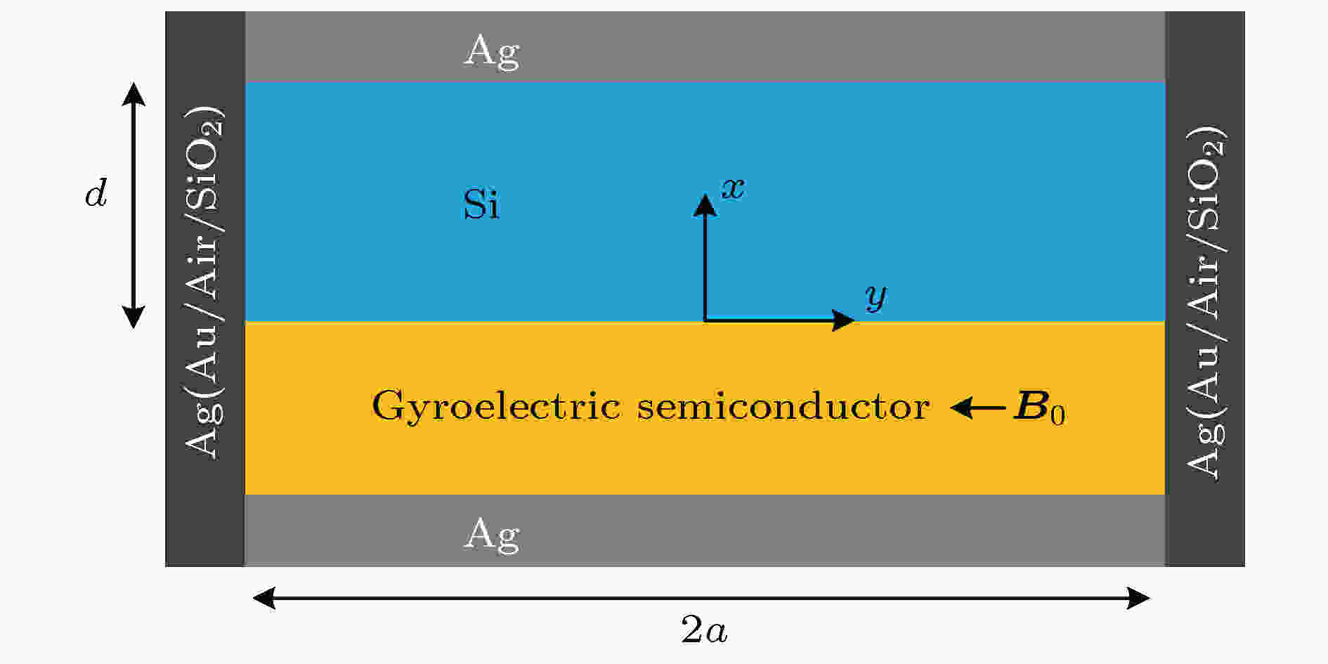
A C-band rectangular waveguide with gyroelectric semiconductor is designed to study the non-reciprocal propagation characteristics of surface magnetoplasmons (SMPs), which are generated by an external magnetic field. The effective refractive index method is used to obtain the effective refractive index and transverse electric field distribution of the waveguide, and a two-dimensional rectangular waveguide is approximately regarded as a combination of two one-dimensional planar waveguides. The dispersion equation of planar waveguide with
$ {\rm{E}}_{mn}^x$
mode in rectangular waveguide is derived. The influences of the structural parameters of rectangular waveguide and the refractive index of material on the non-reciprocal dispersion relation and time-delay characteristics are analyzed by numerical method. Due to the effect of external magnetic field, the off-diagonal elements of dielectric tensor in magnetic photonic crystal are changed. The generation of electrical anisotropy leads the time reversal symmetry to be broken. As a result, the dispersion curves of the rectangular waveguide are asymmetric with respect to propagation constant, and the complete one-way transmission of SMPs can be realized in the asymmetric frequency region. The dispersion curve tends to be a dispersion curve of planar waveguide as the width of rectangular waveguide increases, but the non-reciprocal frequency range is approximately unchanged. The width of the core region and the refractive index of the side material have a significant influence on the non-reciprocal dispersion characteristics: the group velocity of SMPs decreases withωand propagation constant decreasing. The group velocity is related to the waveguide width, propagation constant and the operating wavelength. The relationship between the normalized group velocity and the width of the waveguide separately operating at 1530, 1550 and 1565 nm are studied. The group velocity is relatively slow when the width of waveguide’s core region is between 140 nm and 233.5 nm, and the minimum group velocity reaches 5.43 × 10⁻²c. As for the slow light effect, the rectangular waveguide is better than planar waveguide. The rectangular waveguide has a large engineering tolerance in the width of core region, which is 93.5 nm. In addition, the dispersion curves of the rectangular waveguide with SiO2, Air, Au and Ag as the left and right cladding layers are calculated. As a result, the group velocity is proportional to the refractive index of the side material in theydirection of the rectangular waveguide. The slow light effect is the most obvious when the material is silver, and the minimum transmission speed can reach 2.8 × 10⁻³c.
2019, 68 (15): 154701.
doi:10.7498/aps.68.20190097
Abstract +
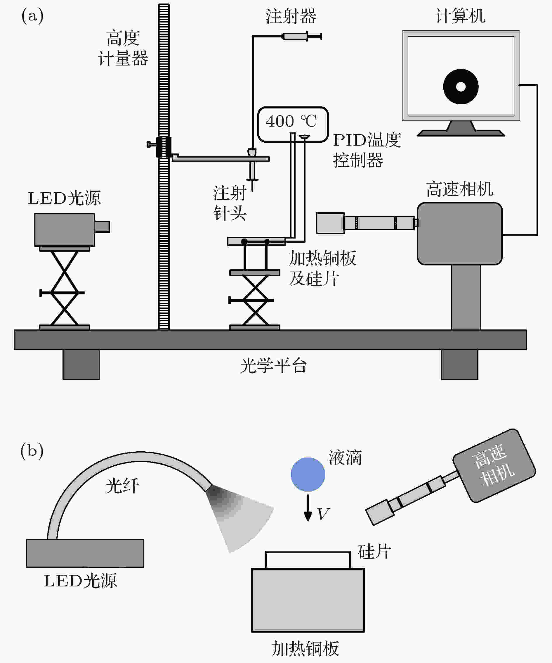
The impact of droplets on surfaces is a ubiquitous phenomenon, and reducing the droplet residence time is the aim of many studies because of the potential applications in self-cleaning, anti-icing, corrosion resistance, etc. This study identifies a mode of droplet bouncing (bouncing-with-spray) that can reduce the residence time significantly. And compared with the way of using complex microstructures on the substrate employed in previous studies, simply heating the substrate to reduce the residence time is novel and simple. The dimensionless residence time decreases down to about 40% compared with that from the traditional retraction-bouncing mode. The reduction in the residence time is due to the burst of vapor bubbles in the liquid film, which results in holes forming in the liquid film and consequently the liquid film recoiling from the holes. The reduction in the recoiling distance leads to the reduction in the recoiling time. Then a simplified theoretical model with considering the energy balance and the critical condition of the bubble burst is proposed. According to this theoretical model, a scaling law is proposed for the transition boundary between the retraction-bouncing mode and the bouncing-with-spray mode in the film boiling regime, and it accords well with our experimental data. This model can also explain the transition boundary between these two modes in the transition boiling regime.
PHYSICS OF GASES, PLASMAS, AND ELECTRIC DISCHARGES

2019, 68 (15): 155201.
doi:10.7498/aps.68.20190610
Abstract +
When ultrashort pulse laser interacts with near-critical-density plasma, extremely strong transient electromagnetic field will generate a great variety of nonlinear phenomena, such as efficient pulse absorption, magnetic self-channeling, nonlinear coherent structure, and electron and ion acceleration. It is of great significance to make a profound study of these physical processes for studying the laser-plasma interaction. Here in this work, we investigate the near-critical-density plasma structure and its temporal evolution by using proton radiography. The plasma is generated by the interaction of ultra-intense femtosecond laser (I
$\sim $
3.6 × 10¹⁸W/cm2) with high-density gas-jet target, which can produce plasma with electron densityne
$ \sim$
0.7nc(here,ncis the near-critical-density) for 800 nm laser. The proton beam is produced by the interaction of another ultra-intense femtosecond laser with stainless steel foil target. In the experiment, the proton beam is split into two asymmetric spots. On the one hand, the distance between two spots first increases rapidly and decreases slowly as time goes by. On the other hand, the size of proton beam spot on the right side is obviously lager than the one on the left side. The modification of proton beam profile indicates that a transient electric field with a maximum amplitude of 109V/m is produced when ultrashort laser pulse interacts with the plasma. Besides, the electric field in the direction of laser propagation axis is stronger than that in the opposite direction. When the proton beam goes through the laser-plasma interaction area, most of the protons enter into the electric field in the direction of laser propagation axis, only a small number of protons enter into the electric field in the opposite direction, resulting in the fact that the proton beam is split into two asymmetric spots. The space-charge field in the plasma is induced by the laser ponderomotive force which expels the electrons piled up into a step-like profile. This field can be sustained for a long time, as the ions expand slowly because of the coulomb repulsion between ions, and the hot electrons continue to move forward with energy of a few MeV. At the end, these expanded ions gradually recombine with the reflowed electrons, causing the space-charge field to weaken until it disappears eventually. As a result, the deflection of the proton beam by the electric field in the plasma is also weakened, so the distance between proton beam splitting spots is correspondingly reduced. The hypothesis is justified by the particle-in-cell simulations. The results may have important implications in laser wake-field electron acceleration, ion acceleration and fast ignition scheme to inertial confinement fusion.
CONDENSED MATTER: STRUCTURAL, MECHANICAL, AND THERMAL PROPERTIES
2019, 68 (15): 156101.
doi:10.7498/aps.68.20190604
Abstract +

EDITOR'S SUGGESTION
2019, 68 (15): 156501.
doi:10.7498/aps.68.20190670
Abstract +
Monolayer of graphene oxide has great potential applications in ion and molecular screening, desalination and purification of water, gas separation, biosensing, proton conductors, lithium batteries, super capacitors and other fields, due to its excellent physical and chemical properties. However, the graphene oxide prepared by chemical and physical methods, such as the commonly used Hummers method is a metastable material. The transformation and regulation of the physical and chemical properties of the final morphology are essential, and systematic research is urgently needed. In this paper, the thermostat treatment method is used to control the metastable transformation of graphene oxide. The relationship of content, type, and morphology with temperature of oxygen-containing graphene oxide are detected by X-ray photoelectron absorption spectroscopy, Fourier infrared absorption spectroscopy, scanning electron microscope, etc.; and the effects of temperature on the stability of solution suspension stability, photon energy band and tensile strength of graphene oxide in the transformation process are analyzed by using Zeta potential, ultraviolet absorption spectrum, tensile force. The quantitative test results show that there exists a phenomenon in which the epoxy phase decreases, the hydroxyl group increases and the overall oxygen content decreases in the metastable transition process of graphene oxide, and the monolayer morphology of graphene oxide does not change significantly in this process. This structural transformation, however, greatly enhances the viscosity and hydrophilicity of the suspension, and remarkably reduces the energy band and considerably raises the tensile strength enhancement effect. When the transformation process is long enough, the hydrophilicity of the graphene oxide will decrease and precipitate. It is indicated that a further dehydration transition occurs between the hydroxyl groups. In addition, in the paper we also analyze the effect of constant temperature treatment time and concentration of suspension on this transformation process. The relevant research results are helpful in understanding the performance change of metastable graphene oxide suspension with temperature, and have certain reference value for the specific application of graphene oxide.
2019, 68 (15): 156801.
doi:10.7498/aps.68.20182189
Abstract +
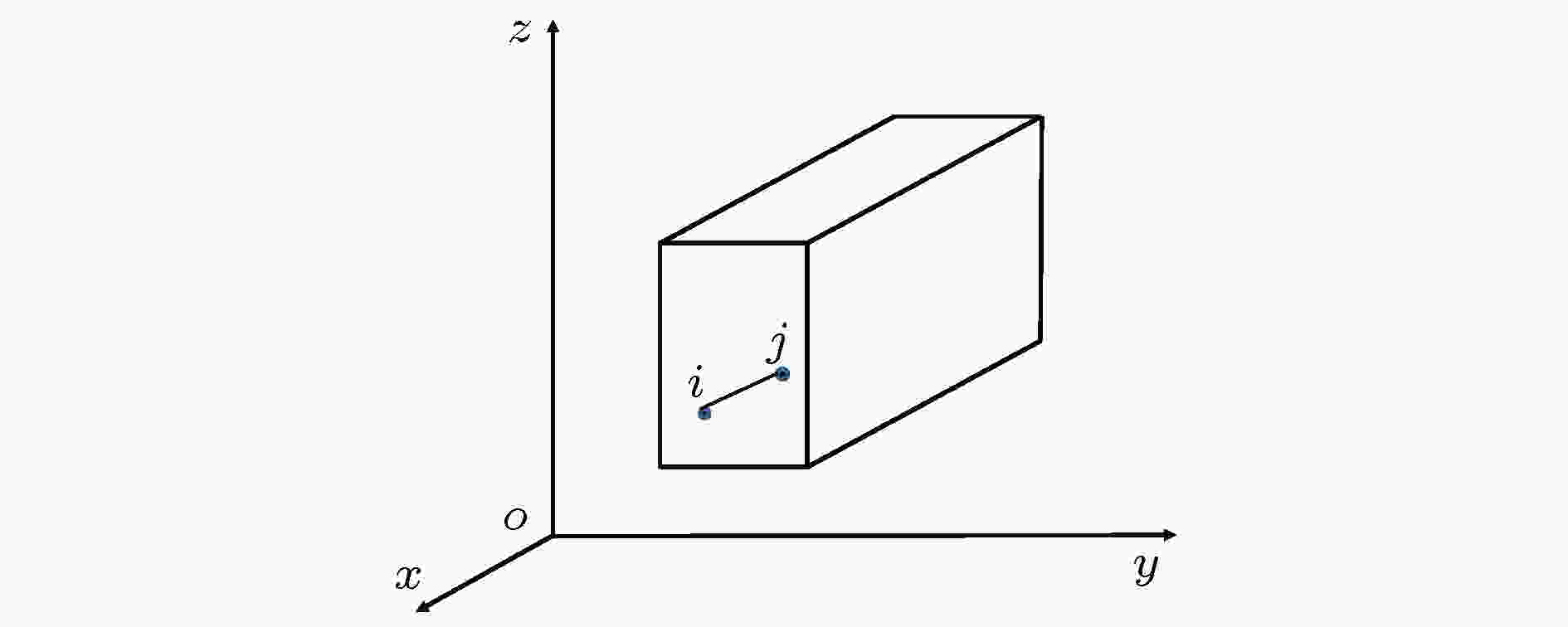
The expression of equilibrium pressure tensor for uniform systems derived from Virial theorem can be divided into two parts: dynamic pressure tensor and configuration pressure tensor. The local mean pressure tensor is obtained by physical analysis of the equilibrium non-uniform system. In this paper, this expression is derived in a more concise way. The theoretical relationship, with undetermined parameters, between the three parts (the volume contribution, the surface contribution and the line contribution) of the average configuration pressure of a homogeneous fluid system and the local average sizeL*with the atomic diameter as length unit greater than 8 is given. Taking argon as an example, molecular dynamics simulation is carried out by using the Lennard-Jones potential between atoms at temperature 180 K and density 0.8 (atomic diameter)–3. The simulation curves of configuration pressure and its three parts are given, and the undetermined coefficients in the theoretical relationship under the condition ofL*> 8 are determined. It is found that forL*> 2, With the increase ofL*, the volume contribution decreases monotonously from the positive pressure to the negative total configuration pressure, while the surface contribution and the line contribution both increase monotonously and tend to zero, but the line contribution tends to zero fastest. The complex characteristics of various behaviors are explained physically. It is concluded that the surface contribution and the line contribution can be neglected only ifL*are large enough. In nanoscale, the neglect of the surface contribution and the line contribution, i.e., the neglect of the boundary effect, will bring obvious errors to the calculation. Finally, molecular dynamics simulation shows that the configuration pressure increases with the increase of temperature. These conclusions are significant for optimizing the selection of pressure tensor in molecular dynamics simulation.
CONDENSED MATTER: ELECTRONIC STRUCTURE, ELECTRICAL, MAGNETIC, AND OPTICAL PROPERTIES
2019, 68 (15): 157201.
doi:10.7498/aps.68.20190213
Abstract +
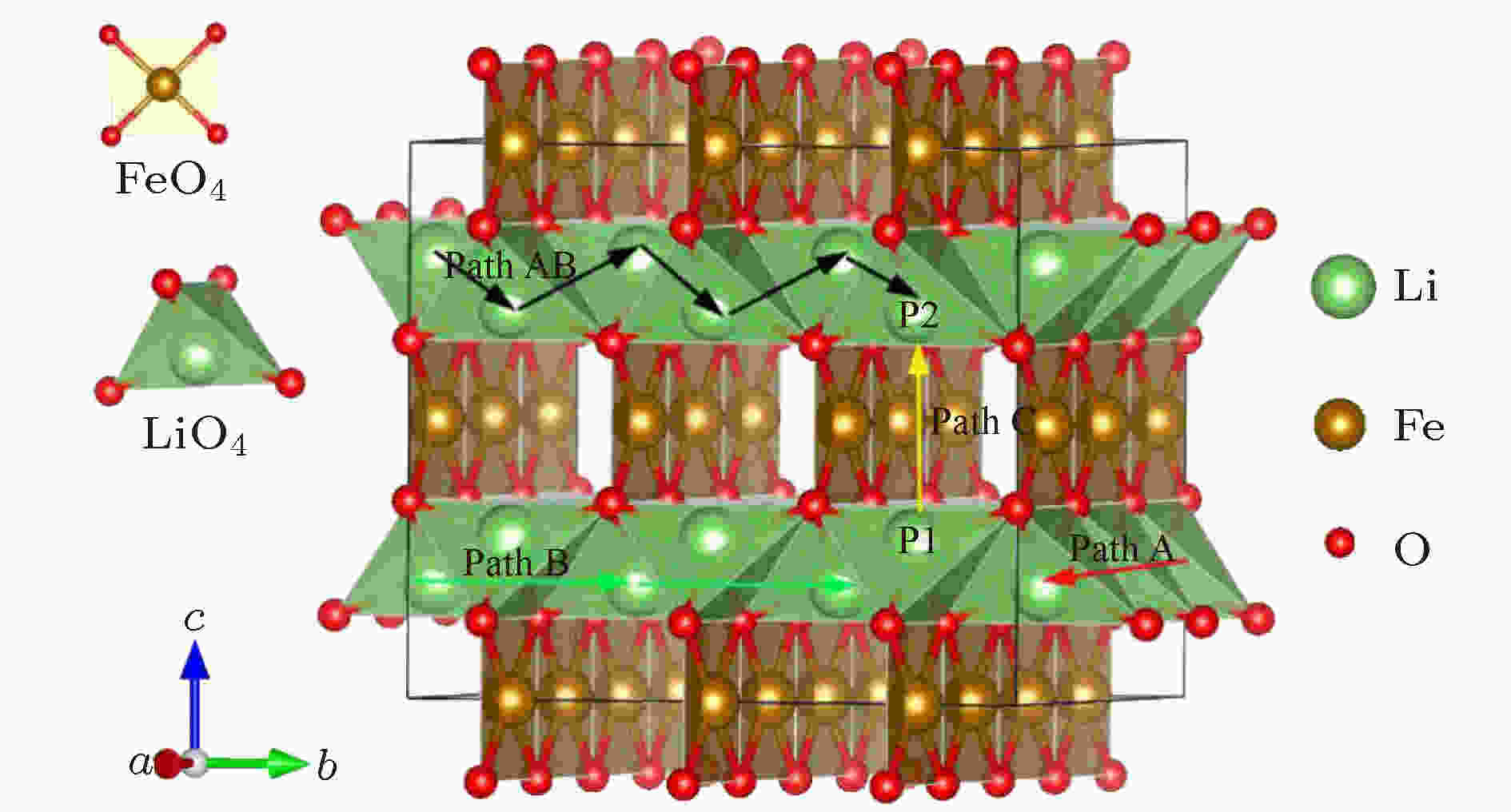
The electronic structures and lithium diffusion in the cathode materialImmm-Li2FeO2of lithium-ion batteries are calculated by the first-principles method based on the density functional theory. The calculated results show thatImmm-Li2FeO2is ferromagnetic, and the band structure indicates a semi-metal character. The d-electrons of Fe ions are in the low spin state, with a spin polarization of 8.01%. The spin-up and spin-down band structure are also analyzed by using thel-decomposed electronic density of states. Furthermore, the energy barriers for the lithium ion diffusion in different directions are calculated by the nudged elastic band method. For comparison, the potential barriers for the Li2MO2(M= Co, Ni, Cu) are also calculated. The results suggest that it is easier for Li ion to diffuse in thec-axis directionof Li2FeO2, with an energy barrier of only 0.1 eV. The energy barrier is 0.21 eV for Li to diffuse in theab-axis direction, while the diffusion barrier is 0.39 eV along thea-axis direction of Li2FeO2. All these values of energy barriers are lower than those in other Fe-based cathodes mentioned, indicating that the Li diffusion coefficient inImmm-Li2FeO2should be larger than those of other materials, which also indicates that the Li2FeO2is of great importance as cathode material.
2019, 68 (15): 157501.
doi:10.7498/aps.68.20190207
Abstract +
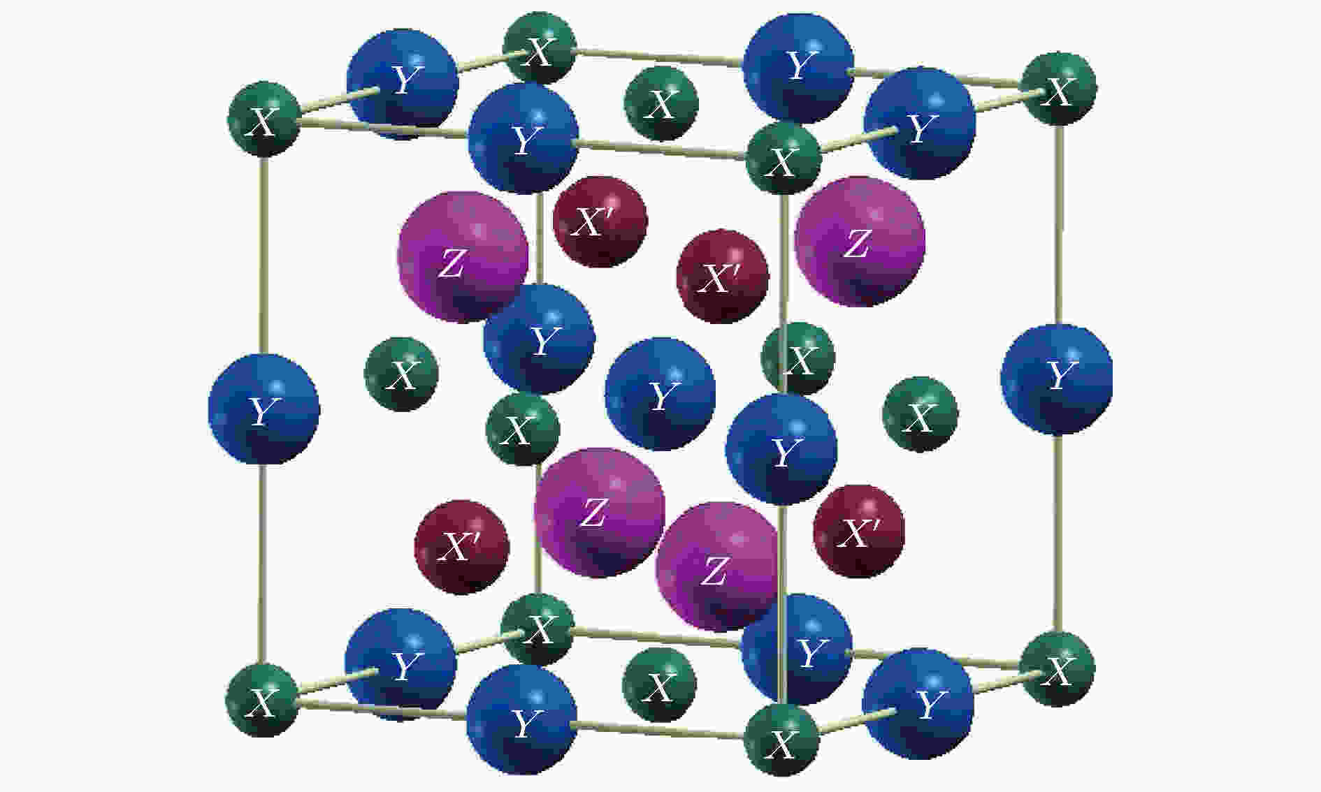
Using the first principle full-potential linearized augmented wave method we study the electronic structure and elastic and magnetic properties of CoMnZnZ(Z= Si, Ge, Sn, Pb) LiMgPdSn-type Heusler alloys. These compounds have the composition CoMnZnZwith 1︰1︰1︰1 stoichiometry, whereZdenotes the main group element Si, or Ge, or Sn, or Pb. The exchange-correlations are treated within the generalized gradient approximation of Perdewe-Burke-Ernzerhof. For each of all studied Heusler alloys, the ferromagnetic state is considered to be more stable than the paramagnetic state, judged by the energy. The total energy of the magnetic calculation is lower than that of the nonmagnetic state for each of all three serise compounds at the equilibrium lattice constant, indicating that the magnetic state is more stable than the nonmagnetic state. We determine the elastic constantsC11,C12andC44, which have not been established previously in experiment nor in theory. The elastic constant indicates the weakened resistance to sheardeformation compared with the resistance to unidirectional compression. We derive other mechanical parameters, i.e., the shear modulusG, Young’s modulusE, Poisson’s ratioν, and shear anisotropic factorA, which are the important elastic moduli for applications. These compounds each have a lower anisotropy and possess a low probability to develop micro-crack or structural defect in its growing process. The sound velocity and Debye temperature for each of the CoMnZnZ(Z= Si, Ge, Sn, Pb) compounds in their stable structure are calculated. The CoMnZnPb exhibits the lowest Debye temperature, and the highest value is observed for CoMnZnGe. The electronic structure calculations show that CoMnZnZ(Z= Si, Ge, Sn) each exhibit a gap in the band of minority states, and they are clearly half-metallic ferromagnets, except for the CoMnZnPb. The CoMnZnZ(Z= Si, Ge, Sn) compounds and their magnetic moments are in reasonable agreement with the Slater-Pauling rule, and they comply with a Slater-Pauling rule ofMt=Zt– 28, which indicates the half metallicity and high spin polarization for these compounds. The CoMnZnSi compound has the largest half-metallic gap value and the gap is about 0.66 eV. The magnetic properties are primarily determined by the Mn atoms, which contribute the highest magnetic moments. The localmoment of theZelement atom is negligibly small. The hybridization of the d orbitals between Co and Mn can explain the origin of the Slater-Pauling rule in half-metallic quaternary Heusler alloys. The half-metallic gap comes mainly from the interaction between the Co and Mn atoms.
2019, 68 (15): 157701.
doi:10.7498/aps.68.20182273
Abstract +
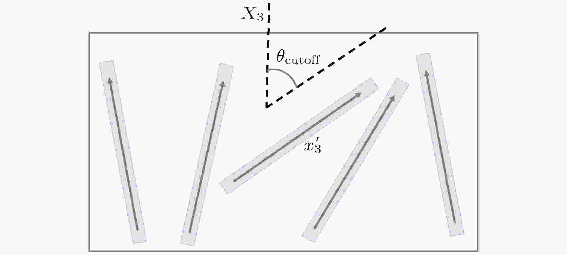
In this paper, a composite physical property calculation software—Composite Studio is developed based on the modified effective medium theory. The computing kernel of the software is written in C++ language and its GUI is designed by Qt. With the development of the computation technique, the material genome project is proposed, which tries to shorten the period of the material design by high-throughput computation, data mining and property database establishment. On a mesoscopic scale, there are several kinds of the models to calculate the physical properties of the composite materials. However, these models usually have the formula in quite a lot of kinds of forms. A general commercial software for physical property calculation on a mesoscopic scale is still leaking. The software uses Green’s function to solve the constitutive equations. It calculates the effects of microstructural factors on physical properties. These factors include volume fraction, aspect ratio of reinforce particles, orientation distribution, and macroscopic orientation. It can obtain more than 10000 composites by freely combining four microstructure factors. The operation process of software includes 5 steps. The first step is to choose the materials of matrix and reinforcement. The second step is to select the shape type of reinforcement. The third step is to set the range of values for the microstructure factors of the composite materials. The fourth step is to choose the calculation model and start calculations. The last step is to plot and analyze the results. In addition, researchers can directly have the calculation results through the single point analysis module of the software. We use several two-dimensional line plots to display multi-dimensional calculation results. This is convenient and efficient for researchers to observe and analyze the results. Until now, two calculation modules were developed in Composite Studio, i.e. the elastic modulus calculation module and the dielectric constant calculation module. The software can be applied to different computer systems. In the future, the Composite Studio can be used as a general-purpose calculation tool embedded into an server platform for popular composite design.
INTERDISCIPLINARY PHYSICS AND RELATED AREAS OF SCIENCE AND TECHNOLOGY
2019, 68 (15): 158101.
doi:10.7498/aps.68.20190350
Abstract +
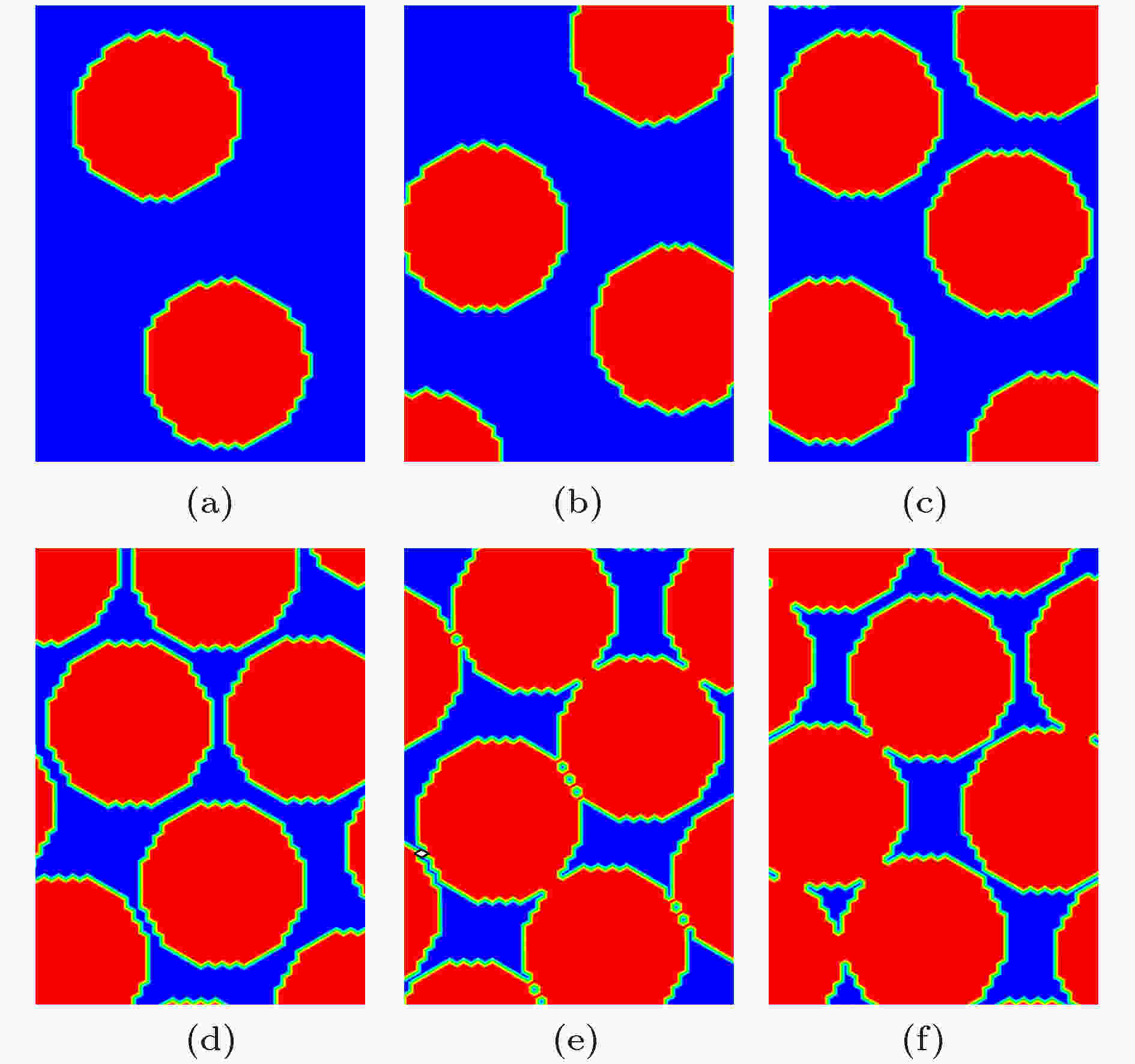
Unlike the ductile materials, the failure seriously limits the strength of the brittle medium. To understand the mechanism of controlling the dynamic impact strength of diamond-SiC superhard composite under shock wave compression, the numerical simulation is conducted with a lattice-spring model that can describe the mechanical properties of diamond-SiC superhard composite quantitatively. For the simulation, the diamond-SiC superhard composite is constructed by different volume content of diamond and SiC particles. The obtainted shock wave profiles indicate that the dynamic impact strength first increases and then decreases with the increase of diamond content in the sample. The analysis based on the meso-scale damage pattern reveals that such a variation of dynamic impact strength corresponds to three damage evolution modes. When the diamond content increases to a value between 10%–50% in volume percentage, the long slip bands are first dominated, and then becomes short slip bands when the diamond content is 70%, and damage happens mainly in SiC matrix whereas most of the diamond particles are not damaged. When the diamond content is above a critical value of 70% in volume percentage, even the short slip bands are limited heavily, which makes it difficult to relax the shear stress on diamond particles and causes serious damage to diamond particles, finally results in the reduction of dynamic strength.
EDITOR'S SUGGESTION
2019, 68 (15): 158201.
doi:10.7498/aps.68.20190431
Abstract +
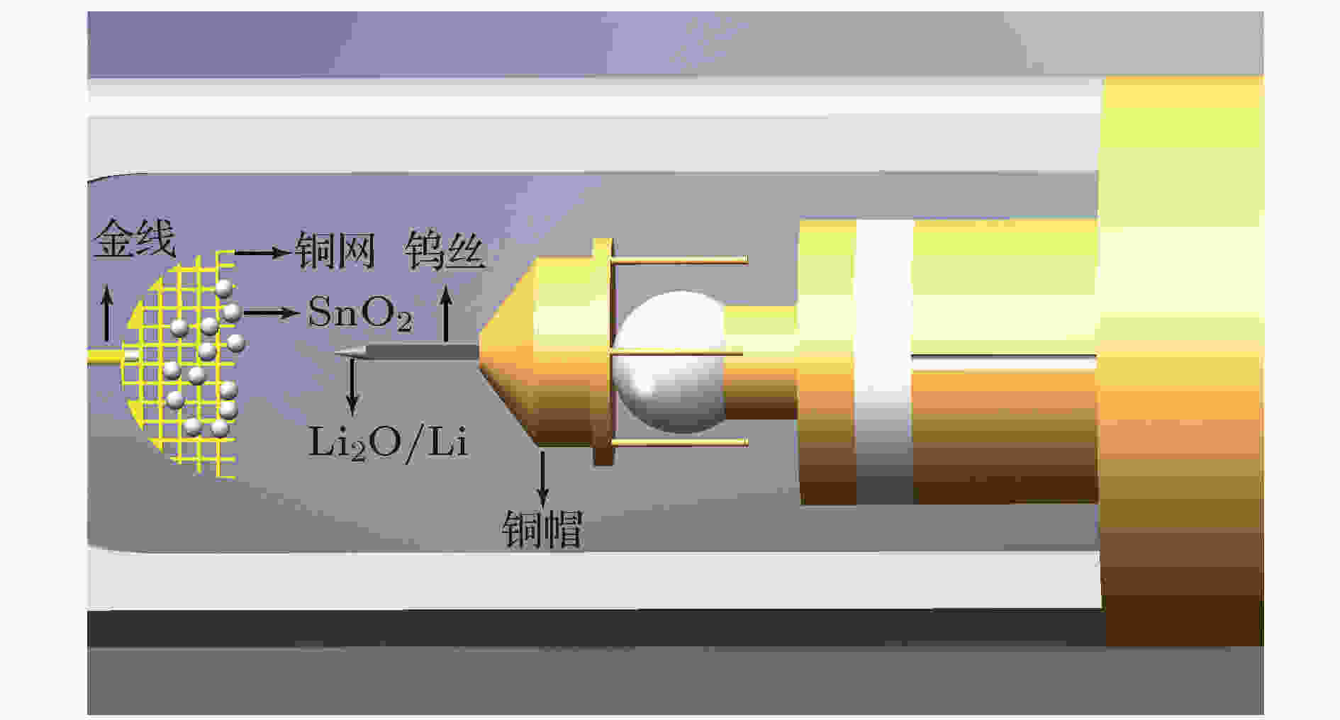
Tin oxide (SnO2) has attracted a lot of attention among lithium ion battery anode materials due to its rich reserves, high theoretical capacity, and safe potential. However, the mechanism of the SnO2nano materials in the lithiation-delithiation reaction, especially whether the first-step conversion reaction is reversible, is still controversial. In this paper, SnO2nanoparticles with an average particle size of 4.4 nm are successfully prepared via a simple hydrothermal method. A nanosized lithium ion battery that enables thein situelectrochemical experiments of SnO2nanoparticles is constructed to investigate the electrochemical behavior of SnO2in lithiation-delithiation process. Briefly, the nanosized electrochemical cell consists of a SnO2working electrode, a metal lithium (Li) counter electrode on a sharp tungsten probe, and a solid electrolyte of lithium oxide (Li2O) layer naturally grown on the surface of metal Li. Then, the whole lithiation-delithiation process of SnO2nanocrystals is tracked in real time. When a constant potential of –2 V is applied to the SnO2with respect to lithium, lithium ions begin to diffuse from one side of the nanoparticles, which is in contact with the Li/Li2O layer, and gradually propagate to the other side. Upon the lithiation, a two-step conversion reaction mechanism is revealed: SnO2is first converted into intermediate phase of Sn with an average diameter of 4.2 nm which is then further converted into Li22Sn5. Upon the delithiation, a potential of 2 V is applied and Li22Sn5phase can be reconverted into SnO2phase when completely delithiated. It is because the interfaces and grain boundaries of nano-sized SnO2may impede the Sn diffusing from one grain into another during lithiation/delithiation and then suppress the coarsening of Sn, and enable the Li2O and Sn to be sufficiently contacted with each other and then converted into SnO2. This work provides a valuable insight into an understanding of phase evolution in the lithiation-delithiation process of SnO2and the results are of great significance for improving the reversible capacity and cycle performance of lithium ion batteries with SnO2electrodes.
2019, 68 (15): 158501.
doi:10.7498/aps.68.20190646
Abstract +
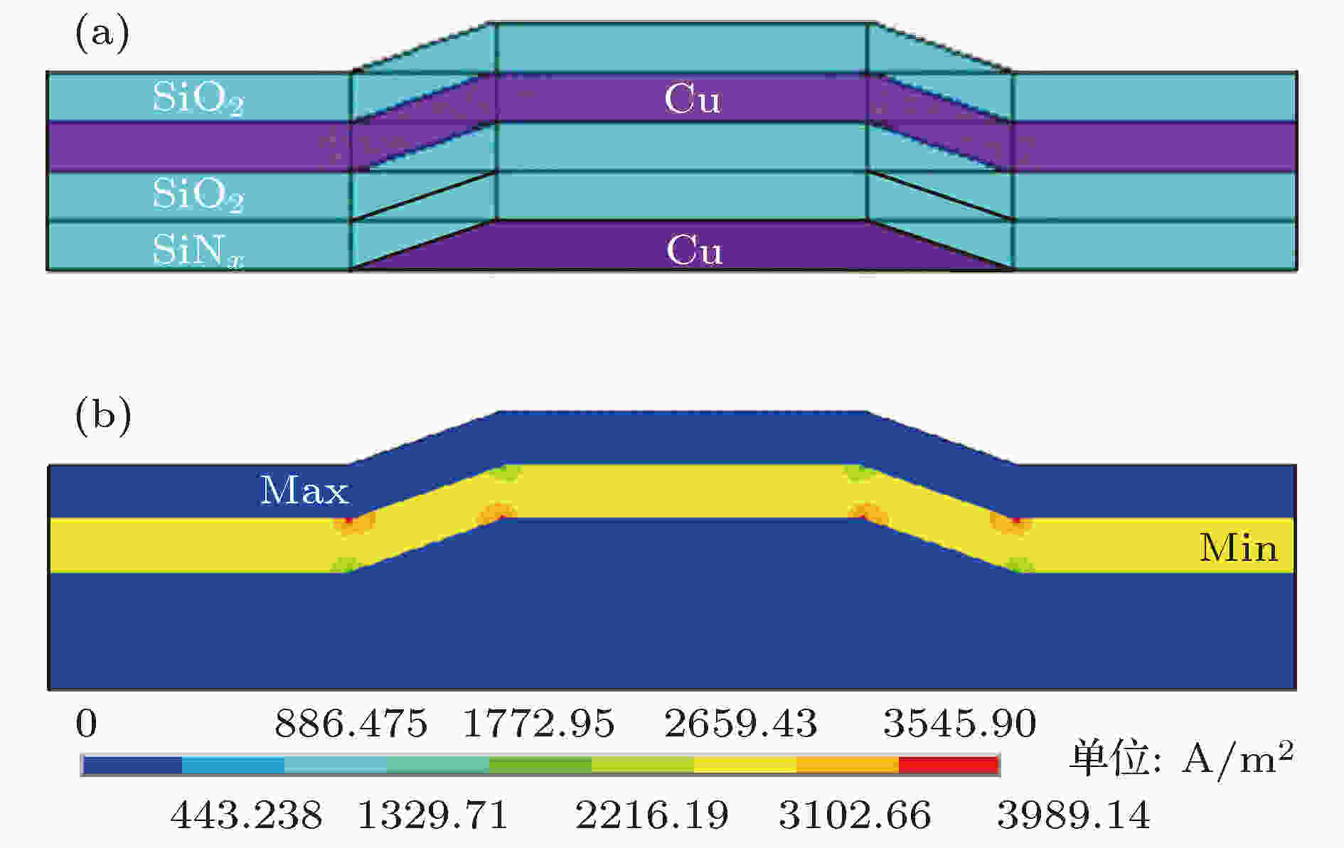
The InGaZnO thin film transistor (IGZO TFT) backplane combined with Cu interconnection has nearly an order of magnitude lower in the ability to withstand voltage than that of traditional a-Si TFT backplane on the production line. The breakdown voltage of Mo/Cu interconnection between data line and gate line is only about 60% of that of traditional a-Si TFT backplane. The electrostatic discharge (ESD) breakdown of Mo/Cu:SiNx/SiO2:Mo/Cu structure has become an important factor affecting the normal display of IGZO TFT ultra high definition (UHD) panel. We find that the anti-ESD damage ability of IGZO TFT devices needs matching with the anti-ESD damage ability of interlayer Cu interconnection in order to achieve a high-robustness IGZO TFT backplane. The position of ESD damage in IGZO TFT backplane is commonly in the climbing place where the data line crosses the scanning line. In this paper, a Cu diffusion model is proposed to explain the mechanism for the ESD failure of interlayer Cu interconnection. The Cu metal in gate line diffuses into SiNx/SiO2gate insulator, and Cu metal at the corner of data line, where the date line crosses the gate line, diffuses into SiO2film on the date line. The selection conditions of three kinds of protection architectures for ESD protection circuits around Cu interconnection, i.e. R-type, R-half-type, and Diode-type protection architectures, are proposed. On the basis of process optimization such as Cu metal film forming and Cu metal interface treatment, an ESD protection method for the Cu interconnection periphery of IGZO TFT backplane with high robustness is proposed. For the stable production process of IGZO TFT, combined with the design window of ESD protection circuit, the peripheral ESD protection circuit of Cu interconnect is designed with diode-type protection circuit on the IGZO TFT backplane of large-sized UHD and QUHD panel, which effectively improves the effect of interlayer Cu interconnection of IGZO TFT backplane on ESD damage. Through the production verification, it is proved that the metal diffusion of Cu interconnection on IGZO TFT backplane is the fundamental reason for reducing the anti-ESD damage ability of Mo/Cu:SiNx/SiO2:Mo/Cu structure. The rationality of the proposed ESD damage model for interlayer Cu interconnection is verified, which provides a theoretical basis for subsequent IGZO TFT backplane design with high robustness.

2019, 68 (15): 158502.
doi:10.7498/aps.68.20190413
Abstract +
Magnetic fields are generally sensed by a device that makes use of the Hall effect. Hall-effect sensors are widely used for proximity switching, positioning, speed detecting for the purpose of control and condition monitoring. Currently, the Hall sensor products are mainly based on the narrow-bandgap Si or GaAs semiconductor, and they are suitable for room temperature or low temperature environment, while the novel wide-bandgap GaN-based Hall sensors are more suitable for the application in various high-temperature environments. However, the spatial structure of the GaN-based sensor is mainly horizontal and hence it is only able to detect the magnetic field perpendicular to it. To detect the parallel field on the sensor surface, the vertical structure device is required despite encountering many difficulties in technology, for example reducing the vertical electric field in the two-dimensional electron gas (2-DEG) channel. The vertical Hall sensor has not been reported so far, so it is technically impossible to realize three-dimensional magnetic field detection on single chip. To address the mentioned issues, in this paper we propose a design of the vertical Hall sensor based on the wide-bandgap AlGaN/GaN heterojunction material, which adopts a shallow etching of 2-DEG channel barrier to form a locally trenched structure. The material parameters and physical models of the proposed device are first calibrated against real device test data, and then the key structural parameters such as device electrode spacing ratio, mesa width and sensing electrode length are optimized by using technology computer aided design, and the device characteristics are analyzed. Finally, the simulation results confirm that the proposed Hall sensor has a higher sensitivity of magnetic field detection and lower temperature drift coefficient (
$\sim $
600 ppm/K), and the device can work stably in a high-temperature (greater than 500 K) environment. Therefore, the vertical and horizontal devices can be fabricated simultaneously on the same wafer in the future, thus achieving a three-dimensional magnetic field detection in various high-temperature environments.
GEOPHYSICS, ASTRONOMY, AND ASTROPHYSICS
2019, 68 (15): 159401.
doi:10.7498/aps.68.20190433
Abstract +
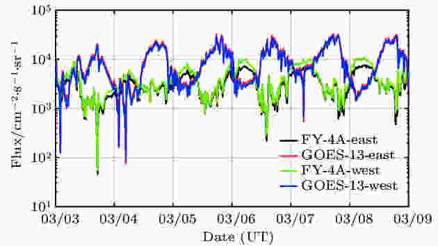
Magnetospheric relativistic electrons can destroy on-orbit spacecrafts completely by internal charging and discharging effects. As the characteristics and physical mechanism of this space particle are still unclear, magnetospheric relativistic electrons have always been an important object of space environment exploration and space science research. For studying the physical mechanisms and developing models relating to magnetospheric relativistic electrons, it is necessary to use the observations from different satellites and detectors at the same time. Eliminating the systematic deviation between different detection systems to assimilate the observations from different sources is essentially required by such researches. In this work, the on-orbit cross-calibration and assimilation for relativistic electron (> 2 MeV) observations from FengYun 4A and GOES-13 are performed. In this work, only the observations obtained under very quiet geomagnetic conditions (Kp< 2) are adopted to ensure that the objects of study are the radiation belt particles, which are stably captured by the geomagnetic field. According to the physical characteristics of the radiation belt particles, that is, the three adiabatic invariants, and based on the Liouville theorem, the phase space density of the stably captured particles is unchanged. In this paper, the relativistic electron flux data of energy > 2 MeV and instrument pitch angle are in the east and west direction respectively. If the particles’ energy is the same, then their correspondingμvalues are the same, and their particles’ directions are the same, then their correspondingJvalues are the same, and the Liouville theorem can be simplified as the drift shellLmis the same, the fluxes are the same, and the electron fluxes observed by the two satellites are compared in the drift shellLmcoordinate. The systematic deviation between the two satellites’ relativistic electronic observations can be obtained. According to this result, the data assimilation is carried out, and the results show that the system deviation can be removed well. By this research work, the systematic deviation between two important relativistic electron detection systems in geosynchronous orbit is obtained. Based on the obtained systematic deviations, the assimilations for observations from the two detection systems are achieved. This work lays a solid foundation for the follow-up theoretical and applied researches, and also provides the methods for on-orbit cross-calibration and observation assimilation which could be referred to when other electronic observations on geosynchronous orbit are dealt with.


