


Most Cited
2024, 73 (4): 048901.
doi:10.7498/aps.73.20231416
Abstract +
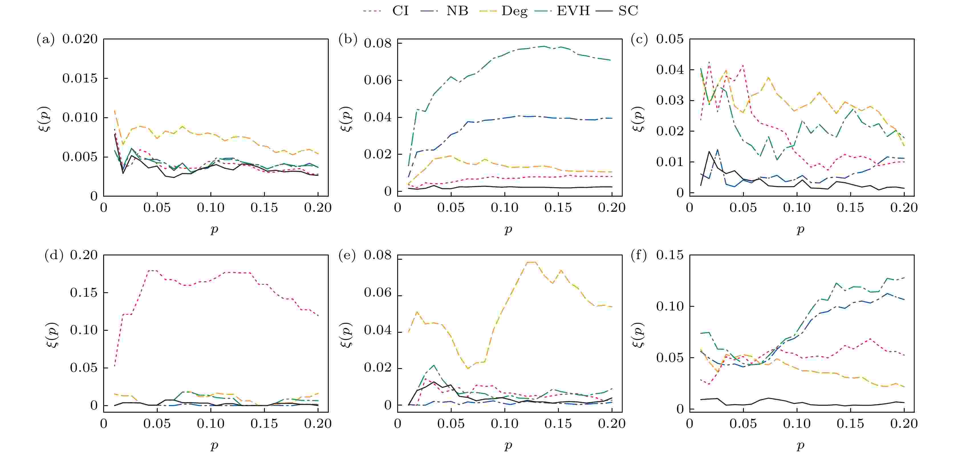
Identifying influential nodes in spreading process in the network is an important step to control the speed and range of spreading, which can be used to accelerate the spread of beneficial information such as healthy behaviors, innovations and suppress the spread of epidemics, rumors and fake news. Existing researches on identification of influential spreaders are mostly based on low-order complex networks with pairwise interactions. However, interactions between individuals occur not only between pairwise nodes but also in groups of three or more nodes, which introduces complex mechanism of reinforcement and indirect influence. The higher-order networks such as simplicial complexes and hypergraphs, can describe features of interactions that go beyond the limitation of pairwise interactions. Currently, there are relatively few researches of identifying influential spreaders in higher-order networks. Some centralities of nodes such as higher-order degree centrality and eigenvector centrality are proposed, but they mostly consider only the network structure. As for identification of influential spreaders, the spreading influence of a node is closely related to the spreading process. In this paper, we work on identification of influential spreaders on simplicial complexes by taking both network structure and dynamical process into consideration. Firstly, we quantitatively describe the dynamics of disease spreading on simplicial complexes by using the Susceptible-Infected-Recovered microscopic Markov equations. Next, we use the microscopic Markov equations to calculate the probability that a node is infected in the spreading process, which is defined as the spreading centrality (SC) of nodes. This spreading centrality involves both the structure of simplicial complex and the dynamical process on it, and is then used to rank the spreading influence of nodes. Simulation results on two types of synthetic simplicial complexes and four real simplicial complexes show that compared with the existing centralities on higher-order networks and the optimal centralities of collective influence and nonbacktracking centrality in complex networks, the proposed spreading centrality can more accurately identify the most influential spreaders in simplicial complexes. In addition, we find that the probability of nodes infected is highly positively correlated with its influence, which is because disease preferentially reaches nodes with many contacts, who can in turn infect their many neighbors and become influential spreaders.

2024, 73 (2): 025201.
doi:10.7498/aps.73.20231056
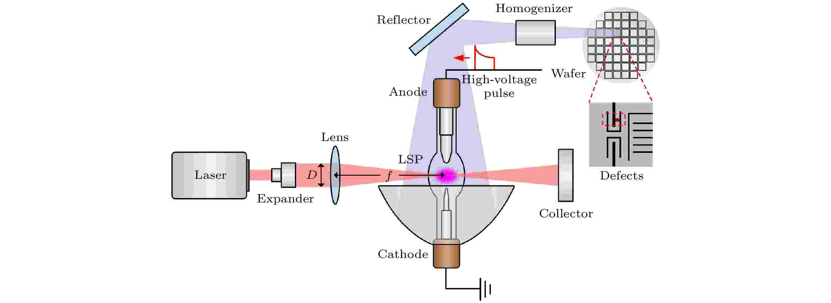
Abstract +
Laser-sustained plasma (LSP), which can be utilized for a novel radiation light source, has advantages such as high irradiance, broad spectral range, and stable emission, demonstrating significant applications in wafer inspection in the field of the semiconductor industry. This paper revisits the historical development of LSP research and introduces fundamental physical processes in LSP. The mathematical description equations for LSP and methods of calculating plasma parameters are provided, thereby a time-dependent two-dimensional fluid model is established by taking into consideration a laser-thermal-hydrodynamic coupling effect. The propagation of the laser in plasma is investigated based on the established model, and the fundamental processes in LSP, including the initial evolution process, laser energy deposition, steady-state characteristics, and instability, are explored. The effectiveness of the simulation model is confirmed through comparing with the experimental results of high-pressure Xe LSP. The findings indicate that the mode, power,F-number of incident lasers, as well as parameters including components, pressure, and flow velocity of gas, can all affect the steady-state properties of LSPs. Under the identical power andF-number conditions, Gaussian mode laser and annular mode laser both produce LSPs with different shapes and positions. Notably, under the conditions of high-power annular laser incidence, large laserF-number, and high flow velocity, the simulation results reveal temporal and spatial instability in LSP. These simulation results contribute significantly to a more in-depth understanding of the underlying physical mechanisms of the LSP. Furthermore, they provide a theoretical basis for designing the light source system and optimizing the multiple parameters. The influence of laser parameters on LSP properties elucidated in this study not only advances the fundamental understanding of LSP but also offers crucial insights for designing and optimizing the light source systems in various applications, particularly in the field of optical detection for semiconductor wafer inspection.
2024, 73 (2): 026102.
doi:10.7498/aps.73.20231357
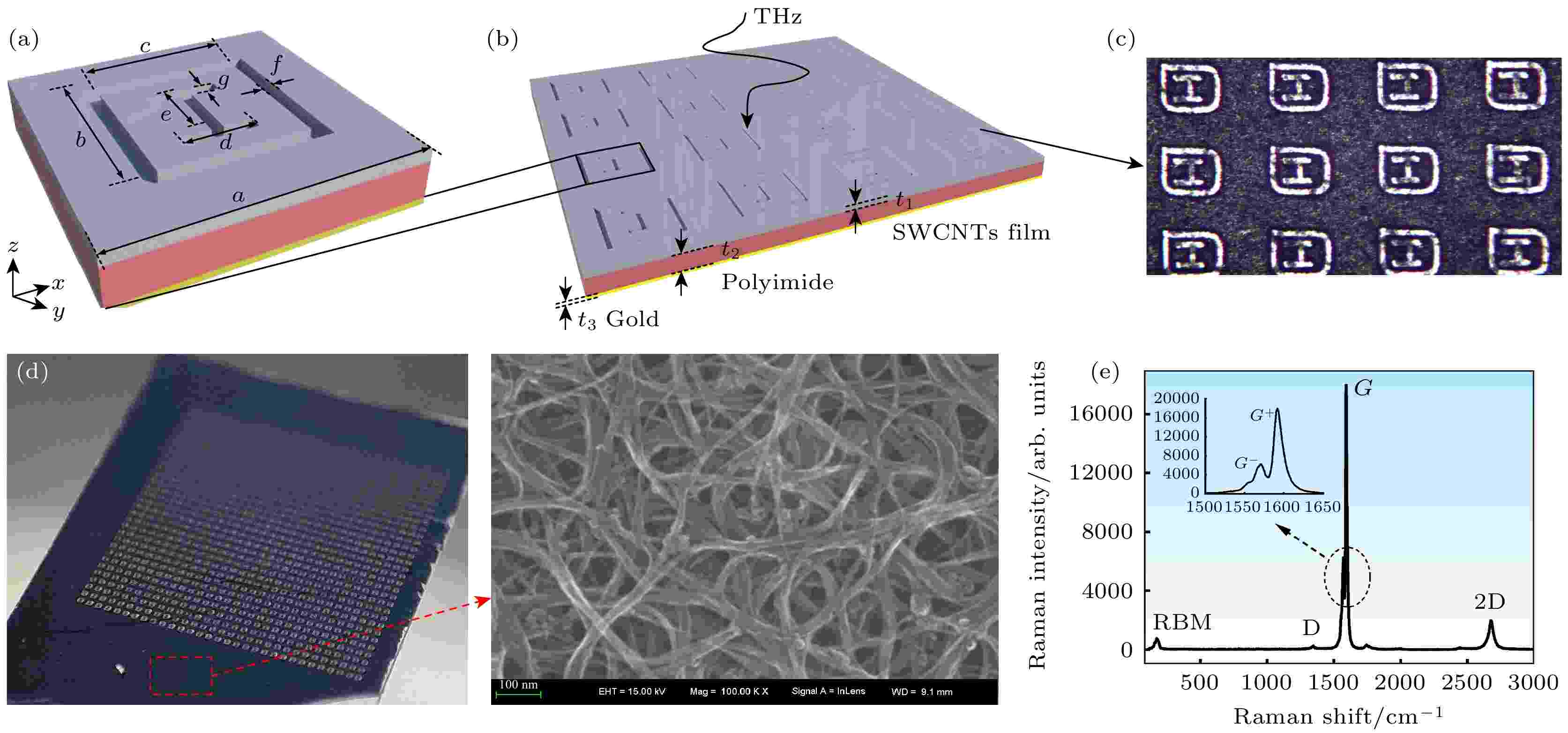
Abstract +
Due to their excellent electrical and optical properties, carbon nanotubes have broad application prospects in the field of optoelectronics. In this work the vacuum filtration method is used to obtain an isotropic single-walled carbon nanotube film by the dispersion of single-walled carbon nanotube powder through vacuum filtration; on the basis of extracting the dielectric parameters of the thin film in a range from 0.4 to 2.0 THz, a novel terahertz metasurface narrowband absorber based on single-walled carbon nanotube films is designed and prepared. This metasurface absorber is composed of square and I-shaped narrow slot resonators. The experimental and simulation results show that the proposed terahertz metasurface absorber exhibits four distinct resonance absorption peaks at 0.65, 0.85, 1.16, and 1.31 THz, respectively, achieving a perfect absorption of up to 90%. The absorption mechanism of this novel multi band terahertz metasurface is elucidated by using the theory of multiple reflection interference. By covering dielectric layers with different refractive indices on the surface of metasurface device, the sensing performance of metasurface acting as refractive index sensor is studied in depth. The research results indicate that this new type of metasurface absorber has high sensitivity for refractive index sensing, providing new ideas and solutions for further developing carbon-based new terahertz metasurface absorbers.
2024, 73 (2): 027703.
doi:10.7498/aps.73.20230708
Abstract +
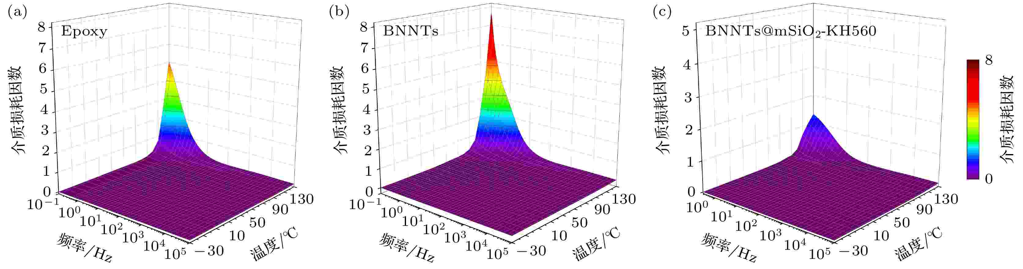
Adding nanofillers into epoxy resin matrices is a common method to achieve their multi-function. Boron nitride nanotubes (BNNTs) with one-dimensional nanostructures have attracted much attention because of their ultra-high thermal conductivity, wide energy level band gap, high aspect ratio and mechanical strength. Yet, the strong π-π non-covalent bonding and lip-lip interactions make BNNTs prone to agglomeration in the epoxy resin matrix. Moreover, the different physicochemical properties of BNNTs and epoxy resins as well as the chemical inertness of BNNTs surface lead to the lack of effective interfacial interaction between BNNTs and epoxy resin matrix. Therefore, the performance of the epoxy composite dielectric is not enhanced by simple blending solely, but will even have the opposite effect. To address the problems of BNNTs, in this study, the surface structure of BNNTs is constructed from the perspective of interface modulation by using sol-gel method to coat mesoporous silica (mSiO2) on BNNTs’ surface and further introducing silane coupling agent (KH560). The results indicate that the surface structure of BNNTs can optimize the level of interfacial interaction between BNNTs and epoxy resin matrix, which leads to stronger interfacial connection and elimination of internal pore phenomenon. The dielectric constant and loss of the composite dielectric prepared in this way are further reduced, reaching 4.1 and 0.005 respectively at power frequency, which is significantly lower than that of pure epoxy resin. At the same time, the mechanical toughness (3.01 MJ/m3) and thermal conductivity (0.34 W/(m⋅K)) are greatly improved compared with the counterparts of pure epoxy resin. In addition, the unique nano-mesoporous structure of mSiO2endows the composite dielectric with a large number of deep traps, which effectively hinders the migration of electrons, thereby improving the electrical strength of the composite dielectric, and the breakdown field strength reaches 95.42 kV/mm. Furthermore, the interfacial mechanism of BNNTs’ surface structure on dielectric relaxation and trap distribution of composite dielectrics is systematically studied by Tanaka multinuclear model. The above results indicate that the good interfacial interaction between BNNTs and epoxy resin matrix is crucial in establishing the micro-interface structure and improving the macroscopic properties of composite dielectrics. This study presents a novel idea for the multifunctionalities of epoxy resin, and also provides some experimental data support for revealing the correlation among surface properties of nano-fillers, microstructure and macroscopic properties of composite dielectric.
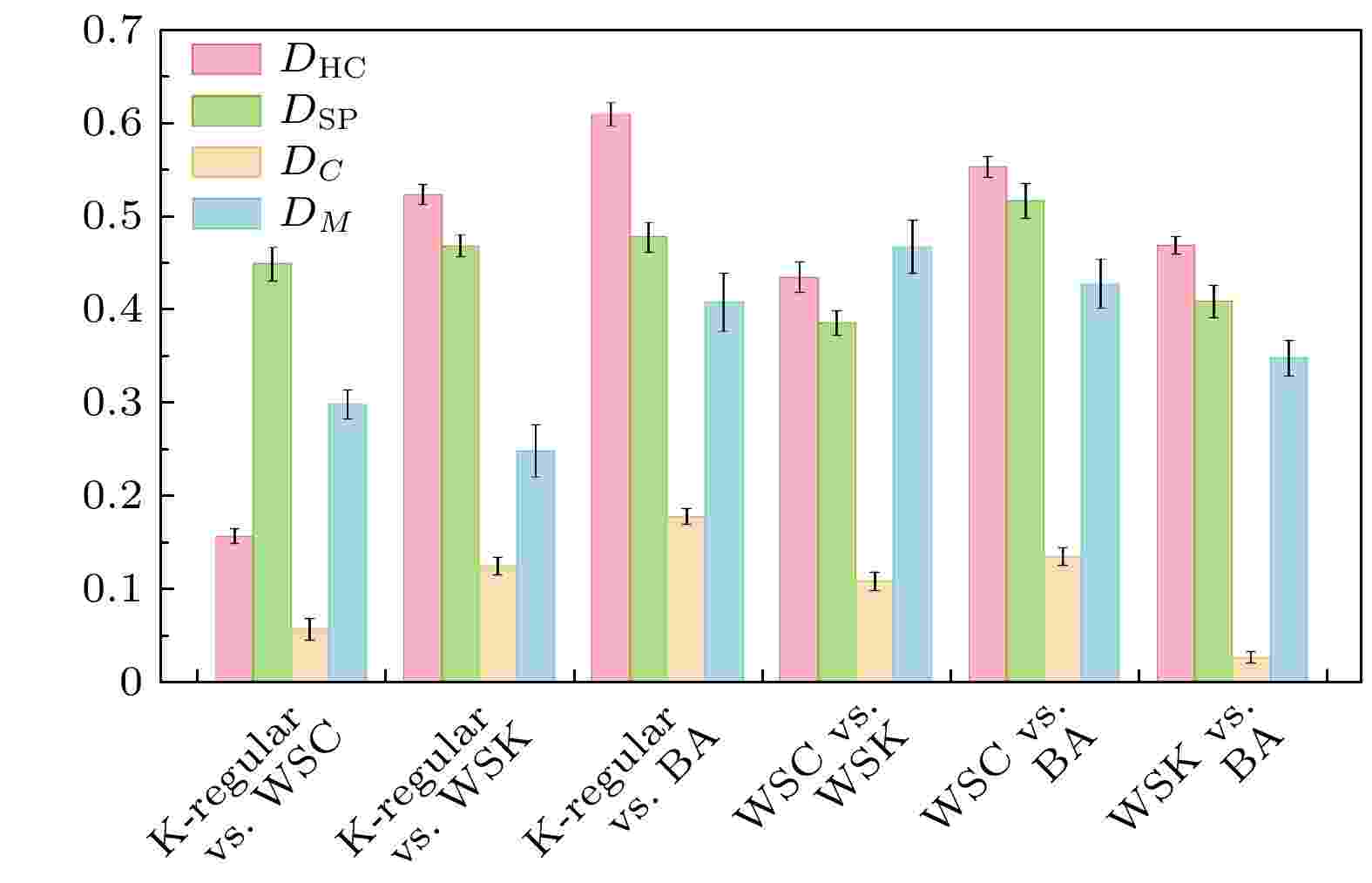
2024, 73 (3): 038901.
doi:10.7498/aps.73.20231096
Abstract +
Quantifying structural similarity between complex networks presents a fundamental and formidable challenge in network science, which plays a crucial role in various fields, such as bioinformatics, social science, and economics, and serves as an effective method for network classification, temporal network evolution, network generated model evaluation, etc. Traditional network comparison methods often rely on simplistic structural properties such as node degree and network distance. However, these methods only consider the local or global aspect of a network, leading to inaccuracies in network similarity assessments. In this study, we introduce a network similarity comparison method based on the high-order structure. This innovative approach takes into account the global and the local structure of a network, resulting in a more comprehensive and accurate quantification of the network difference. Specifically, we construct distributions of higher-order clustering coefficient and distance between nodes in a network. The Jensen-Shannon divergence, based on these two distributions, is used to quantitatively measure the similarity between two networks, offering a more refined and robust measure of network similarity. To validate the effectiveness of our proposed method, we conduct a series of comprehensive experiments on the artificial and the real-world network, spanning various domains and applications. By meticulously fine-tuning the parameters related to three different artificial network generation models, we systematically compare the performances of our method under various parameter settings in the same network. In addition, we generate four different network models with varying levels of randomization, creating a diverse set of test cases to evaluate the robustness and adaptability of the method. In artificial networks, we rigorously compare our proposed method with other baseline techniques, consistently demonstrating its superior accuracy and stability through experimental results; in real networks, we select datasets from diverse domains and confirm the reliability of our method by conducting extensive similarity assessments between real networks and their perturbed reconstructed counterparts. Furthermore, in real networks, the rigorous comparison between our method and null models underscores its robustness and stability across a broad spectrum of scenarios and applications. Finally, a meticulous sensitivity analysis of the parameters reveals that our method exhibits remarkable performance consistency across networks of different types, scales, and complexities.
2024, 73 (1): 017501.
doi:10.7498/aps.73.20231589
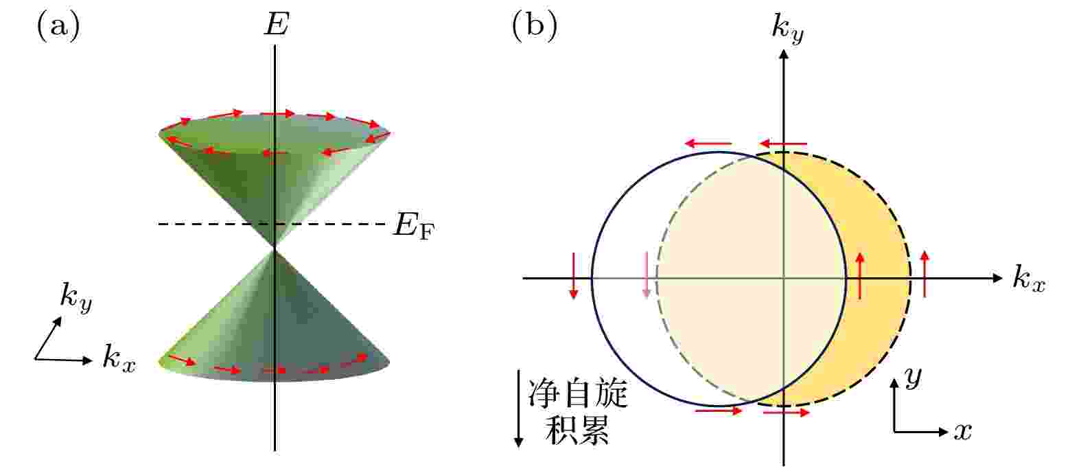
Abstract +
Hall effect is an ancient but highly potential subfield in condensed matter physics, and its origin can be traced back hundreds of years. In 1879, Hall made a momentous discovery that when a current-carrying conductor is placed in a magnetic field, the Lorentz force pushes its electrons to one side of the conductor. This intriguing phenomenon was dubbed Hall effect. Since then, a series of novel Hall effects have been discovered, including anomalous Hall effect, quantum Hall effect, spin Hall effect, topological Hall effect, and planar Hall effec. Notably, Hall effects play an important role in realizing the information transport, since it can realize the mutual conversion of current in different directions. In bosonic systems such as magnons, a series of magnon Hall effects have been found, jointly driving the development of the magnon-based spintronics. In this perspective, we review the researches of the Hall effect in magnonic system in recent years, and briefly introduce its modern semi-classical theories, including virtual electromagnetic field theory and scattering theory. Furthermore, we introduce the different magnon Hall effects and clarify the physics behind them. Finally, the prospect of magnon Hall effect is discussed.

2024, 73 (5): 055202.
doi:10.7498/aps.73.20231679
Abstract +
Laser plasma instability is one of the difficulties that plague inertial confinement fusion. Broadband laser, as an effective tool for suppressing laser-plasma instabilities, has received a lot of attention in recent years. However, the nonlinear bursts of high-frequency instabilities, such as stimulated Raman scattering driven by broadband laser in the kinetic regime, make the suppression effect less than expected. In this study, a broadband laser model with intensity modulation is proposed. By choosing an appropriate intensity modulation envelope, it is possible to interrupt the amplification process of backscattered light in strong pulses, reduce the probability of high-intensity pulses inducing intense bursts, and drastically reduce the fraction of backscattered light and hot electron yield. Numerical simulations show that the intensity-modulated laser has a good ability to suppress stimulated Raman scattering. For a broadband laser with average power of
$ 1.0 \times {10}^{15}\;{\mathrm{W}}/{\mathrm{c}}{{\mathrm{m}}}^{2} $
and a bandwidth of 0.6%, the reflectivity decreases by an order of magnitude and the fraction of hot electron energy above 20 keV decreases from 7.34% to 0.31% by using the intensity modulation technique. The above results confirm the feasibility of using the intensity-modulated broadband laser to suppress the high-frequency instability and are expected to provide a reference for designing the subsequent broadband laser-driven fusion experiments.

2024, 73 (1): 017505.
doi:10.7498/aps.73.20231166
Abstract +
Novel quantum materials such as topological materials, two-dimensional materials, create new opportunities for the spintronic devices. These materials can improve the charge-spin conversion efficiency, provide high-quality interface, and enhance the energy efficiency for spintronic devices. In addition, they have rich interactions and coupling effects, which provides a perfect platform for finding new physics and novel methods to control the spintronic properties. Many inspiring results have been reported regarding the research on topological materials and two-dimensional materials, especially the layered topological and two-dimensional magnetic materials, and their heterostructures. This paper reviews the recent achievements of these novel quantum materials on spintronic applications. Firstly the breakthroughs that topological materials have been made in spin-orbit torque devices is introduced, then two-dimensional magnetic materials and their performances in spintronic devices are presented, finally the research progress of topological materials/two-dimensional magnetic materials heterostructures is discussed. This review can help to get a comprehensive understanding of the development of these novel quantum materials in the field of spintronics and inspire new ideas of research on these novel materials.
2024, 73 (2): 024201.
doi:10.7498/aps.73.20231365
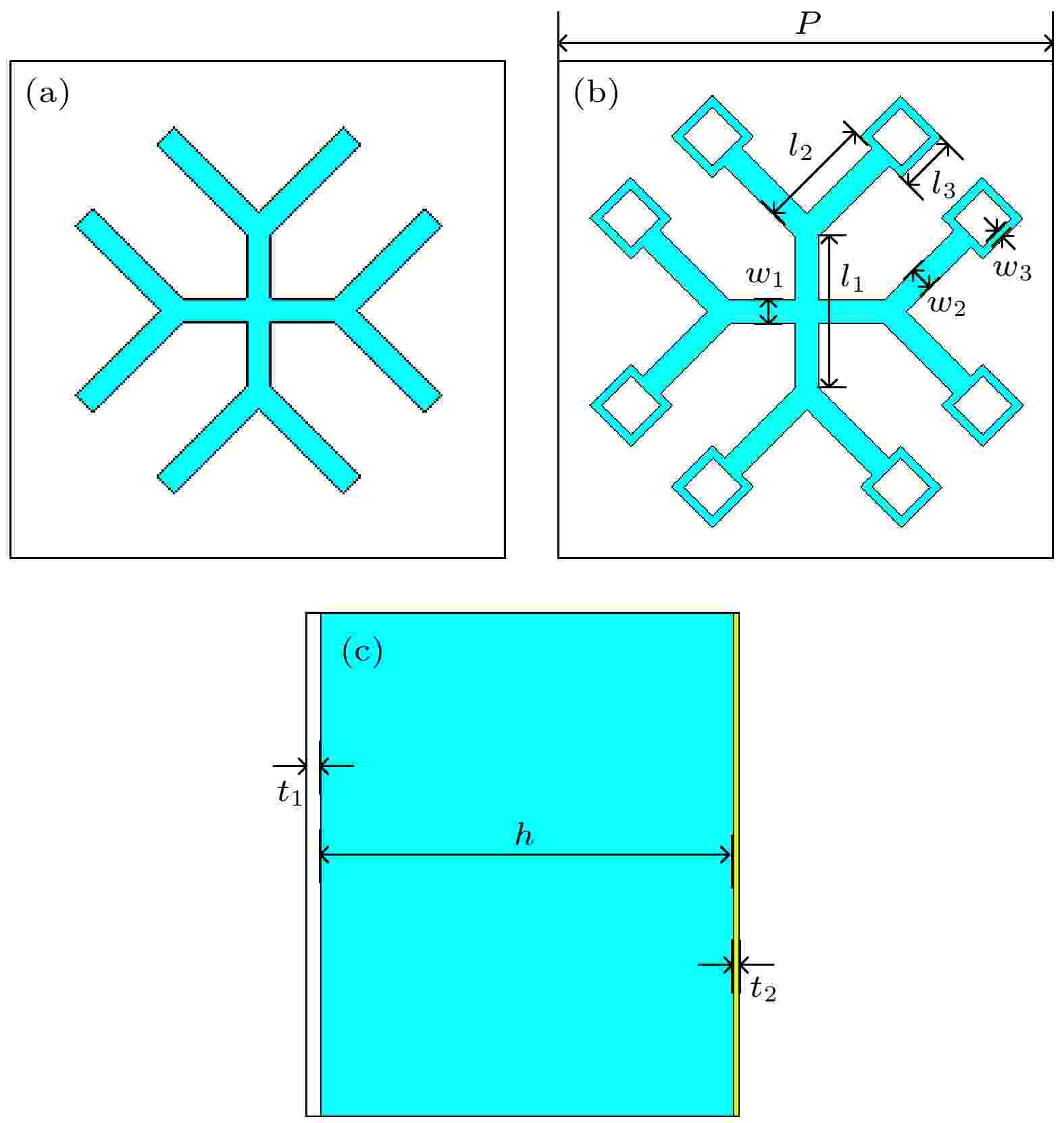
Abstract +
The design of thin frequency selective surface (FSS) absorber based on resistive film that meets the requirements of broadband, polarization independence, incident angle stability, and strong absorption is a challenging task. Fabrication tolerance of resistive film can result in fluctuations in sheet resistance, which negatively affects the absorber performance. To tackle these problems, this work firstly investigates how sheet resistance fluctuations affect the absorbing performance of resistive film FSS absorber. The analysis of simulated surface current density distribution and impedance reveals that the diversity of current paths provides an effective way to mitigate the influence of sheet resistance fluctuation. This is achieved by enabling flexible variation of surface current in response to sheet resistance fluctuations. Consequently, the variation of input impedance of the FSS absorber due to the fluctuation of sheet resistance is suppressed within a small range. Then, a method of extending bandwidth is proposed by employing the complementary variation of FSS impedance with frequency at different layers. By combining this approach with a miniaturization design, a thin and light FSS absorber is developed that exhibits ultra-wide bandwidth, polarization independence and angle stability while mitigating the effects of sheet resistance perturbation. The proposed FSS absorber achieves a 90% absorption bandwidth from 1.50 GHz to 20.50 GHz, covering Ku, X, C, S bands and part of the L and K bands, with a relative bandwidth reaching 173%. The absorber has a thickness of 0.093λLfor both transverse electric (TE) polarization and transverse magnetic (TM) polarization, yielding a figure of merit (FoM, the ratio of the theoretical minimum thickness to the actual thickness) of 0.95, indicating that the thickness is close to the theoretical limit. The absorber maintains over 90% absorption rate for TM polarization at an incidence angle of up to 70°, and 80% absorption for TE polarization at 45°. Furthermore, the 90% absorbance bandwidth of the absorber remains at 167.0% when the sheet resistance of any FSS layer fluctuates within a range from 12 to 30 Ω/sq. A prototype of the proposed FSS absorber is fabricated and measured, and the experimental results are in good agreement with the simulation results, thus validating the effectiveness of the proposed method.
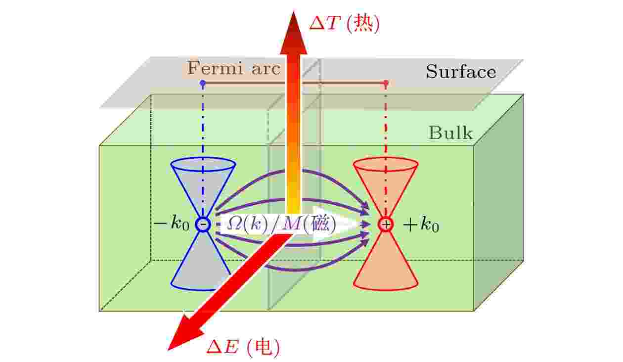
Coupling between magnetism and topology: From fundamental physics to topological magneto-electronics
2024, 73 (1): 017103.
doi:10.7498/aps.73.20231711
Abstract +
Magnetism and topological physics are both well-developed disciplines, and their combination is a demand and foundation for the development of next-generation magneto-electronics. Magnetic topological materials are important products of coupling between magnetic order and topological physics, providing material carrier and regulatory degrees of freedom for novel topological physics. Magnetic Weyl semimetals realize Weyl fermion states under time-reversal symmetry breaking, leading to a host of novel magnetic, electric, thermal, and optical effects through enhanced Berry curvature originating from topology. The interaction between Weyl electrons and magnetic order also establishes topological electronic physics as a new principle and driving force for magneto-electronic applications. At present, the primary task and characteristic of the first development stage of magnetic topological materials is to discover new states and effects, while the understanding of interaction between topologically nontrivial electrons in momentum space and magnetic order in real space has received attention of researchers. The comprehensive advances of these two stages will accumulate the physical foundation and application explorations for topological magneto-electronics. This paper focuses on the two development stages of magnetic topological materials and discusses three aspects: (i) proposal and realization of strategy for magnetic topological materials; (ii) exploration of electronic states with nontrivial topology under uniform magnetic order and their associated novel physical properties; (iii) the interaction between localized magnetic states and topological electrons. It provides an in-depth discussion on current hot topics and development trends in the field, and future development in topological magneto-electronics, thereby assisting in the future development of topological spin quantum devices.
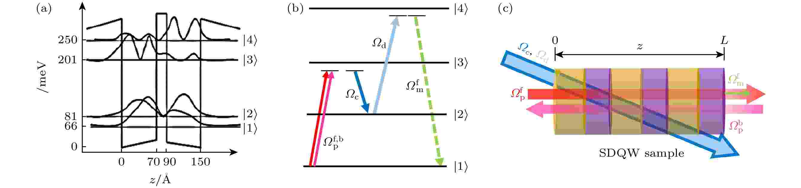
2024, 73 (1): 014201.
doi:10.7498/aps.73.20231212
Abstract +
Optical nonreciprocity has been a popular research topic in recent years. Semiconductor quantum wells (SQWs) play a key role in many high-performance optoelectronic devices. In this paper, we propose a theoretical scheme to achieve nonmagnetic optical nonreciprocity based on the four-wave mixing effect in SQW nanostructures. Using the experimentally available parameters, the nonreciprocal behavior of the probe field in forward direction and backward direction is achieved through this SQW, where both nonreciprocal transmission and nonreciprocal phase shift have high transmission rates. Furthermore, by embedding this SQW nanostructure into a Mach-Zender interferometer, a reconfigurable nonreciprocal device based on high transmission nonreciprocal phase shift that can be used as an isolator or a circulator, is designed and analyzed. The device can be realized as a two-port optical isolator with an isolation ratio of 92.39 dB and an insertion loss of 0.25 dB, and as a four-port optical circulator with a fidelity of 0.9993, a photon survival probability of 0.9518 and a low insertion loss with suitable parameters. Semiconductor media have the advantages of easier integration and tunable parameters, and this scheme can provide theoretical guidance for implementing nonreciprocal and nonreciprocal photonic devices based on semiconductor solid-state media.
2024, 73 (3): 034301.
doi:10.7498/aps.73.20231472
Abstract +
Acoustic scattering is an important part of ocean acoustics, and the acoustic scattering caused by the unevenness of the seafloor surface is one of the reasons for the fluctuation of acoustic propagation in the ocean. In order to solve the acoustic scattering problem of sea bottom surface roughness, normal wave theory is used to model the acoustic field. To simplify the problem, Lambert’s law is used to establish the seafloor rough scattering model in horizontal layered shallow sea waveguides, and the scattering field is assumed to be isotropic in the horizontal direction. Based on this model, the amplitude distribution and the phase distribution of the scattered sound pressure are obtained, and the intensity of the scattered sound field and its spatial correlation coefficient are simulated numerically. The prediction of the scattered sound field under rough interface conditions is realized, and the variation of the spatial characteristics of the scattered sound field with the roughness of the seafloor is revealed. The results show that when Lambert’s law is used to describe the rough interface acoustic scattering and when the seafloor roughness is smaller than the wavelength, the spatial correlation coefficient of the scattered sound field at two different positions in space has a change rule of periodic oscillation attenuation with the increase of spatial distance, and in the vertical direction, the oscillation period is larger and the attenuation is slower. When the roughness increases, the oscillation amplitude of the horizontal and the vertical correlation coefficient gradually increase, the oscillation period of the horizontal correlation coefficient gradually decreases, and the vertical correlation coefficient no longer attenuates in the direction near the seafloor, which is the result of the weakening of the seafloor acoustic scattering. The model theory in this paper can also be extended to the acoustic scattering modeling of rough sea surface. For the case of non-horizontal seabed, the scattered sound field of the rough interface in the waveguide can be obtained by using coupled normal wave or adiabatic normal wave theory.
2024, 73 (5): 054401.
doi:10.7498/aps.73.20231415
Abstract +
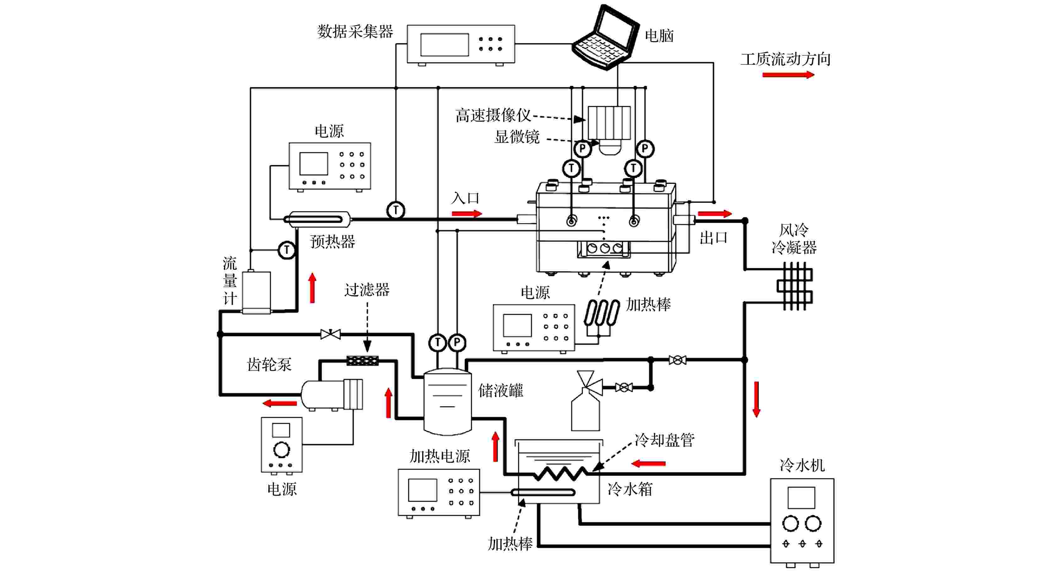
With the rapid development of microelectronic technology, the integration and power of chip are increasing. Heat dissipation with high heat flux in limited space has become a bottleneck restricting the efficient and stable operation of the microelectronic devices. Flow boiling in microchannel heat sink is one of the most essential candidates for solving this problem. It has been shown that remarkable high heat transfer performance can be achieved through the liquid-to-vapor change process, which can dissipate a large amount of heat from a small area. In addition, dielectric fluorinated fluids, such as HFE-7100, HFE-7200, and FC-72, are especially suitable for cooling microelectronic devices, because of their excellent safety and environmental characteristics. However, dielectric fluorinated fluids have poorer thermophysical properties than water. Thus, the flow boiling heat transfer characteristics of dielectric fluorinated fluids can be different from those of water. In this work, flow boiling heat transfer and flow characteristics of HFE-7100 in a rectangular parallel microchannel are investigated. The tests are conducted at mass fluxes from 88.9 to 277.8 kg·m–2·s–1, inlet subcooling temperature from 20.5 to 35.5 ℃ and effective heat flux from 12 to 279 kW·m–2at nearly atmospheric pressure. The effects of mass flux, inlet subcooling temperature, effective heat flux and vapor quality are examined and analyzed. Additionally, flow visualization is also obtained to explain the heat transfer mechanism during the experiments. The results show that the boiling hysteresis is observed for HFE-7100 at low inlet subcooling temperature, and the increasing inlet subcooling temperature and mass flux can delay the onset of nucleate boiling. The increases of inlet subcooling temperature and mass flux can enhance the two-phase heat transfer coefficient. And the two-phase heat transfer coefficient is significantly dependent on the inlet subcooling temperature in the slug flow, while it is significantly dependent on the mass flux in the annular flow. The two-phase pressure drop increases drastically as the effective heat flux increases. And the two-phase pressure drops with different mass fluxes at constant vapor quality are obviously different between the slug flow and the annular flow. Furthermore, the experimental data are compared with four predicted values of the literature. It is found that the correlation of Lockhart has the best statistical agreement with an MAE of 19.6% and over 85% of points in the deviation bandwidth of ±30%. The results in this paper give valuable theoretical guidance for designing and optimizing heat dissipation equipment for microelectronic devices. By utilizing HFE-7100 as the coolant and microchannel heat sinks in flow boiling, it is possible to enhance the stability and reliability of the electronic devices. Additionally, the heat transfer performance associated with different heat fluxes can be improved by regulating the inlet subcooling and mass flow rate. Finally, the two-phase pressure drop correlation proposed by Lockhart can be employed to predict the pump power for heat dissipation equipment.
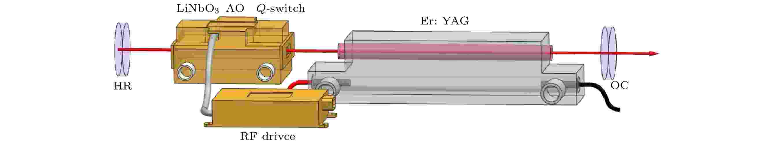
2024, 73 (4): 044205.
doi:10.7498/aps.73.20231616
Abstract +
The 2.94 μm nanosecond erbium laser is an important solid-state laser source in the wide-tuning mid-infrared laser and clinical medical research. In this work, a novel LiNbO3acousto-opticallyQ-switched Er:YAG laser is developed, and the effects of differentQ-switched delay times and output coupler’s reflectivities on the laser output pulse characteristics are investigated at a repetition frequency of 20 Hz. A concave-convex resonant cavity is designed to compensate for the thermal lens effect, and a singleQ-switched pulse is obtained. The maximum pulse energy and minimum pulse duration are 34.68 mJ and 119.9 ns respectively, with corresponding peak power of 289.24 kW. Compared with the plane-plane cavity, the cavity proposed herein increases the output energy by 2.09 times. To our knowledge, this is the highest energy ever obtained in the acousto-opticallyQ-switched Er:YAG laser. This work provides a new means for further studying wide-tuning mid-infrared laser technology.
2024, 73 (4): 047801.
doi:10.7498/aps.73.20231301
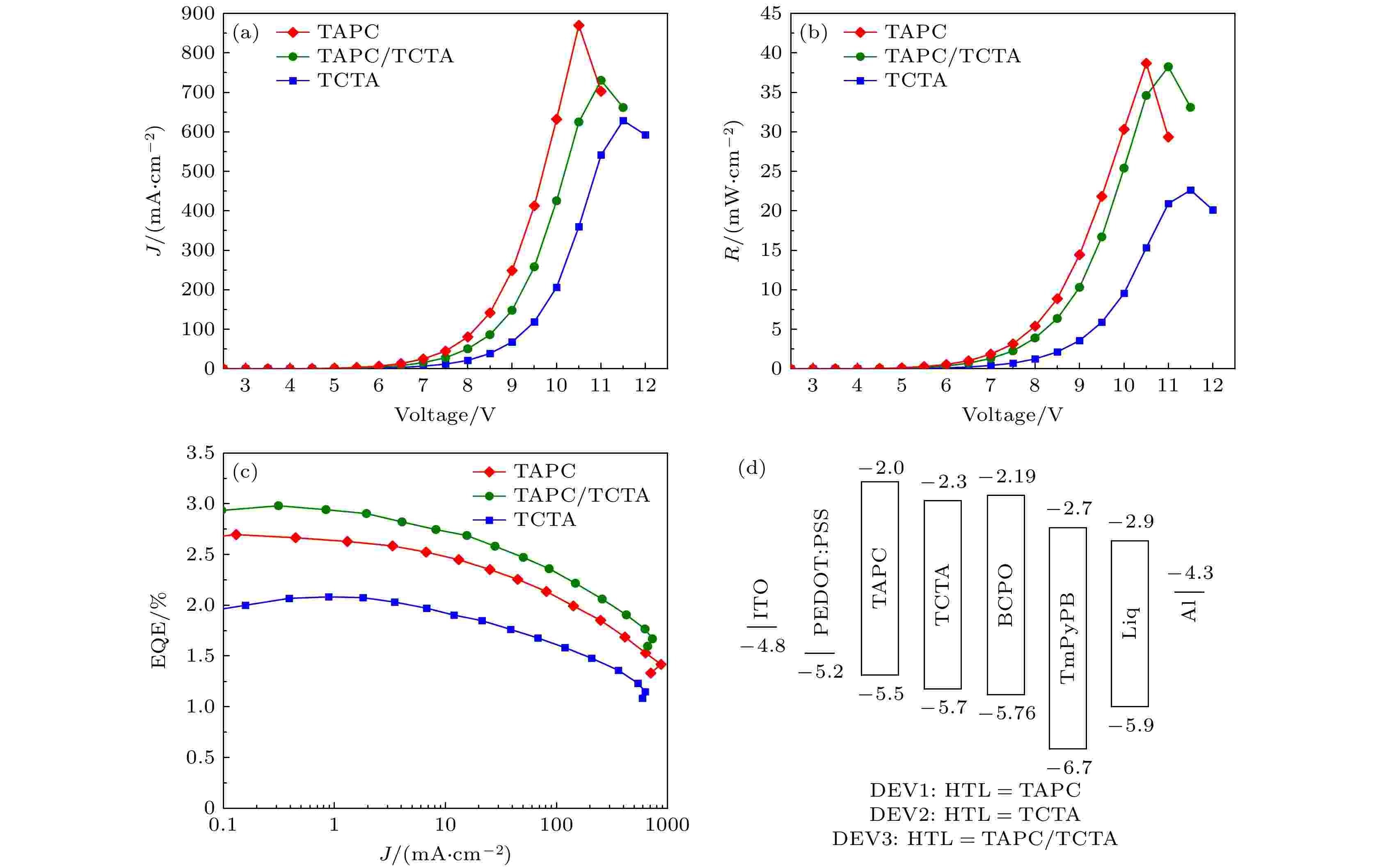
Abstract +
To date, in the traditional method of obtaining near-ultraviolet (NUV) light, mercury atoms, which can create a highly toxic heavy metal contaminant, have been used. Therefore, it is an important issue to obtain NUV light by using new environmentally friendly devices. In the last decade, the fabrication of near ultraviolet organic light-emitting diodes (NUV-OLEDs) has become a research hotspot in the field of organic electronics. However, when the electroluminescence wavelength is extended to shorter than 400 nm, higher requirements are put forward for the materials used for each functional layer in these devices. In this work, a wide bandgap small molecule material of BCPO is used as the luminescent layer. The electron-transporting and hole-transporting materials are determined based on the overlaps between absorption spectra of these materials and emission spectrum of BCPO. And NUV-OLEDs with electroluminescent peak wavelength at 384 nm are prepared. By using the optimal device structure, the maximum external quantum efficiency of the device reaches 2.98%, and the maximum radiance of the device reaches 38.2 mW/cm2. In the electroluminescence spectrum, NUV light with wavelengths below 400 nm accounts for 57% of the light emission. In addition, the device demonstrates good stability when biased at two different constant voltage modes. The multiple key factors which affect the stability of the device are analyzed in detail. Firstly, it is found that the high glass transition temperature (Tg) of hole-transporting material is very important for the long-time stability of this device. The poor device stability is closely related to the lowTgtemperature of hole-transporting material. Secondly, due to the widespread use of PEDOT:PSS as hole injection material in OLEDs, the electron leakage from the hole-transpor layer into the PEDOT:PSS layer may cause significant damage to the conducting polymer. When bombarded with low energy electrons, bond breakage occurs on the surface of PEDOT:PSS, followed by the release of oxygen and sulfur, resulting in changes in conductivity and oxidation reactions with molecules of hole transport material. Thirdly, the photoelectrical stability of organic molecules is the most fundamental reason that restricts the device lifetime. The aging process of material or device is directly relevant to the bond dissociation energy (BDE) of organic molecule. Generally, the BDE value of organic molecule is not high enough. As a result, molecules are prone to chemical bond breakage during electrochemical or photochemical aging. In summary, highly stable NUV-OLEDs should be fabricated by using hole-transporting materials with highTgtemperature, sufficient electron-blocking capacity, and large BDE value.
2024, 73 (2): 027702.
doi:10.7498/aps.73.20230614
Abstract +

2024, 73 (1): 010501.
doi:10.7498/aps.73.20231211
Abstract +
A physical memristor has an asymmetric tight hysteresis loop. In order to simulate the asymmetric tight hysteresis curve of the physical memristor more conveniently, a fractional-order diode bridge memristor model with a bias voltage source is proposed in this paper, which can continuously regulate the hysteresis loop. Firstly, based on fractional calculus theory, a fractional order model of a diode bridge memristor with a bias voltage source is established, and its electrical characteristics are analyzed. Secondly, by integrating it with the Jerk chaotic circuit, a non-homogeneous fractional order memristor chaotic circuit model with a bias voltage source is established, and the influence of bias voltage on its system dynamic behavior is studied. Once again, a fractional-order equivalent circuit model is built in PSpice and validated through circuit simulation. The experimental results are basically consistent with the numerical simulation results. Finally, the experiments on the circuit are completed in LabVIEW to validate the correctness and feasibility of the theoretical analysis. The results indicate that the fractional order memristor with bias voltage source can continuously obtain asymmetric tight hysteresis loop by adjusting the voltage of the bias voltage source. As the bias power supply voltage changes, the non-homogeneous fractional order memristor chaotic system exhibits that the period doubling bifurcation turns into chaos due to the symmetry breaking.
2024, 73 (4): 045201.
doi:10.7498/aps.73.20231369
Abstract +
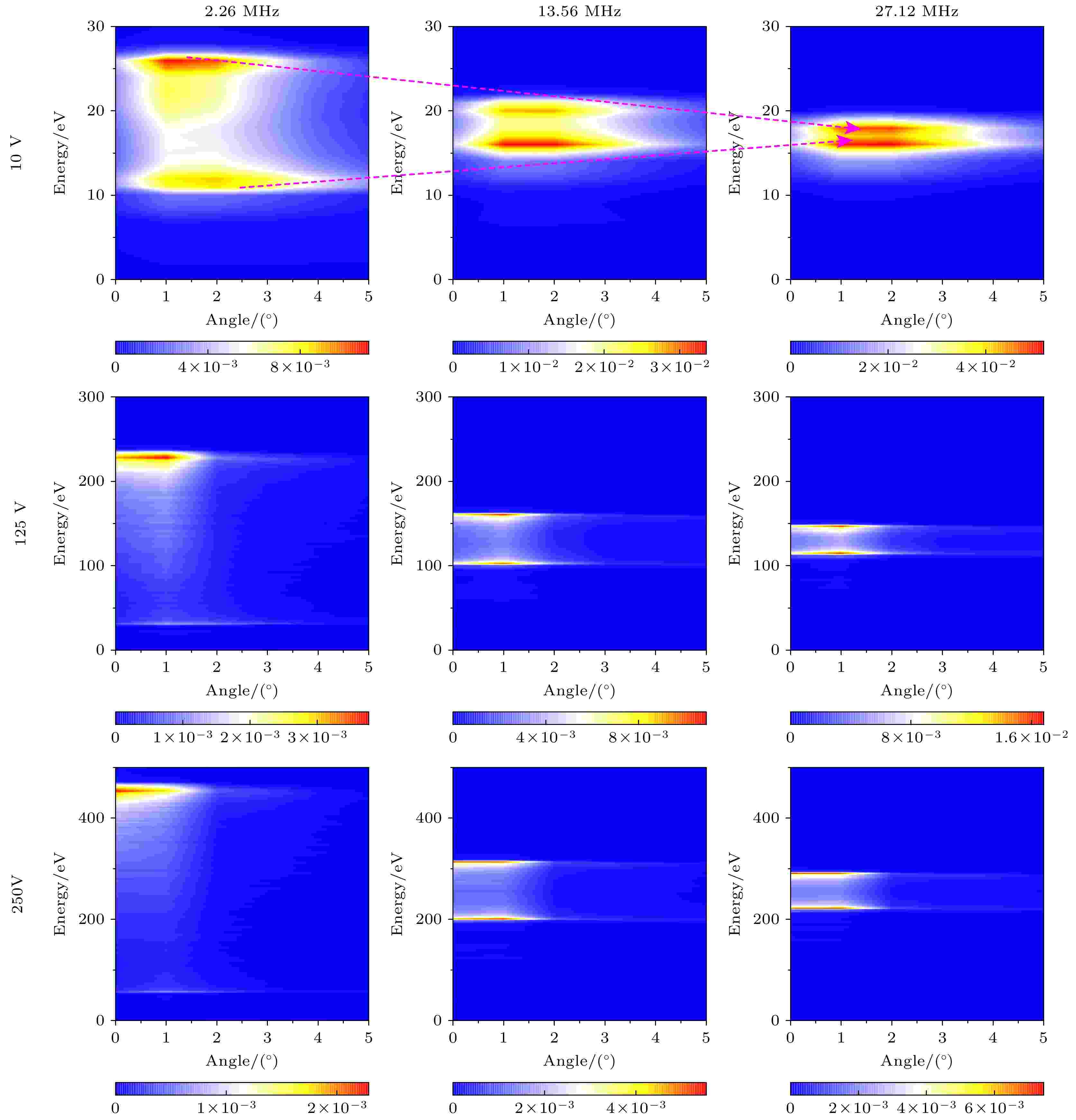
In the etching process, a bias source is usually applied to the substrate of the inductively coupled plasma (ICP) to realize independent modulation of the ion energy and ion flux. In this work, a hybrid model, i.e. a global model combined bi-directionally with a fluid sheath model, is employed to investigate the plasma properties and ion energy distribution function (IEDF) in biased inductively coupled Ar/O2/Cl2plasmas. The results indicate that at a bias frequency of 2.26 MHz, the Cl–ion density and ClO+ion density first increase with bias voltage rising, and then they decrease, and finally they rise again, which is different from the densities of other charged species, such as O and Cl atoms. At the bias frequency of 13.56 MHz and 27.12 MHz, except Cl–and
$ {\text{Cl}}_2^ + $
ions, the evolutions of other species densities with bias voltage are similar to the results at lower bias frequency. The evolution of the species densities with bias frequency depends on the bias voltage. For instance, in the low bias voltage range (< 200 V), the densities of charges species, O and Cl atoms increase with bias frequency increasing due to a significant increase in the heating of the plasma by the bias source. However, when the bias voltage is high, say, higher than 300 V, except
$ {\text{Cl}}_2^ + $
and Cl–ions, the densities of other charged species, O and Cl atoms first decrease with bias frequency increasing and then they increase due to a decrease and then an increase in the heating of the plasma by the bias source. In addition, as the bias frequency increases, the peak separation of IEDF becomes narrow, the high energy peak and low energy peak approach each other and they almost merge into one peak at high bias frequency. The results obtained in this work are of significant importance in improving the etching process.


2024, 73 (3): 037202.
doi:10.7498/aps.73.20231393
Abstract +
In this work, we numerically study the localization properties in a quasi-periodically modulated one-dimensional cross-stitch lattice with a flat band. When
$\varDelta\neq0$
, it is found that there are two different quasi-periodic modulation frequencies in the system after the local transformation, and the competing modulation by two frequencies may lead to the reentrant localization transition in the system. By numerically solving the fractal dimension, the average inverse participation ratio, and the average normalized participation ratio, we confirm that the system can undergo twice localization transitions. It means that the system first becomes localized as the disorder increases, at some critical points, some of the localized states go back to the delocalized ones, and as the disorder further increases, the system again becomes fully localized. By the scalar analysis of the normalized participation ratio, we confirm that reentrant localization stably exists in the system. And the local phase diagram is also obtained. From the local phase diagram, we find that when
$1.6<\varDelta<1.9$
, the system undergoes a cascade of delocalization-localization-delocalization-localization transition by increasingλ. When
$\varDelta=0$
, there exists only one quasi-periodic modulation frequency in the system. And we analytically obtain the expressions of the mobility edges, which are in consistence with the numerical studies by calculating the fractal dimension. And the system exhibits one localization transition. This work could expand the understanding of the reentrant localization in a flat band system and offers a new perspective on the research of the reentrant localization transition.


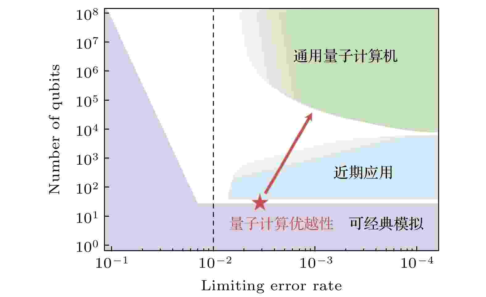
2024, 73 (1): 010301.
doi:10.7498/aps.73.20231795
Abstract +
In the early decades of the 20th century, the inception of quantum mechanics catalyzed the first quantum revolution, resulting in groundbreaking technological advances, such as nuclear energy, semiconductors, lasers, nuclear magnetic resonance, superconductivity, and global satellite positioning systems. These innovations have promoted significant progress in material civilization, fundamentally changed the way of life and societal landscape of humanity. Since the 1990s, quantum control technology has made significant strides forward, ushering in a rapid evolution of quantum technologies, notably exemplified by quantum information science. This encompasses domains such as quantum communication, quantum computing, and quantum precision measurement, offering paradigm-shifting solutions for enhancing information transmission security, accelerating computational speed, and elevating measurement precision. These advances hold the potential to provide crucial underpinning for national security and the high-quality development of the national economy. The swift progression of quantum information technology heralds the advent of the second quantum revolution. Following nearly three decades of concerted efforts, China’s quantum information technology field as a whole has achieved a leap. Specifically, China presently assumes a prominent international role in both the research and practical application of quantum communication, leading the global domain in quantum computing, and achieving international preeminence or advanced standing across various facets of quantum precision measurement. Presently, it is imperative to conduct a comprehensive assessment of the developmental priorities in the realm of quantum information in China for the forthcoming 5 to 10 years, in alignment with national strategic priorities and the evolving landscape of international competition. This will enable the proactive establishment of next-generation information technology systems that are secure, efficient, autonomous, and controllable.

- 1
- 2


