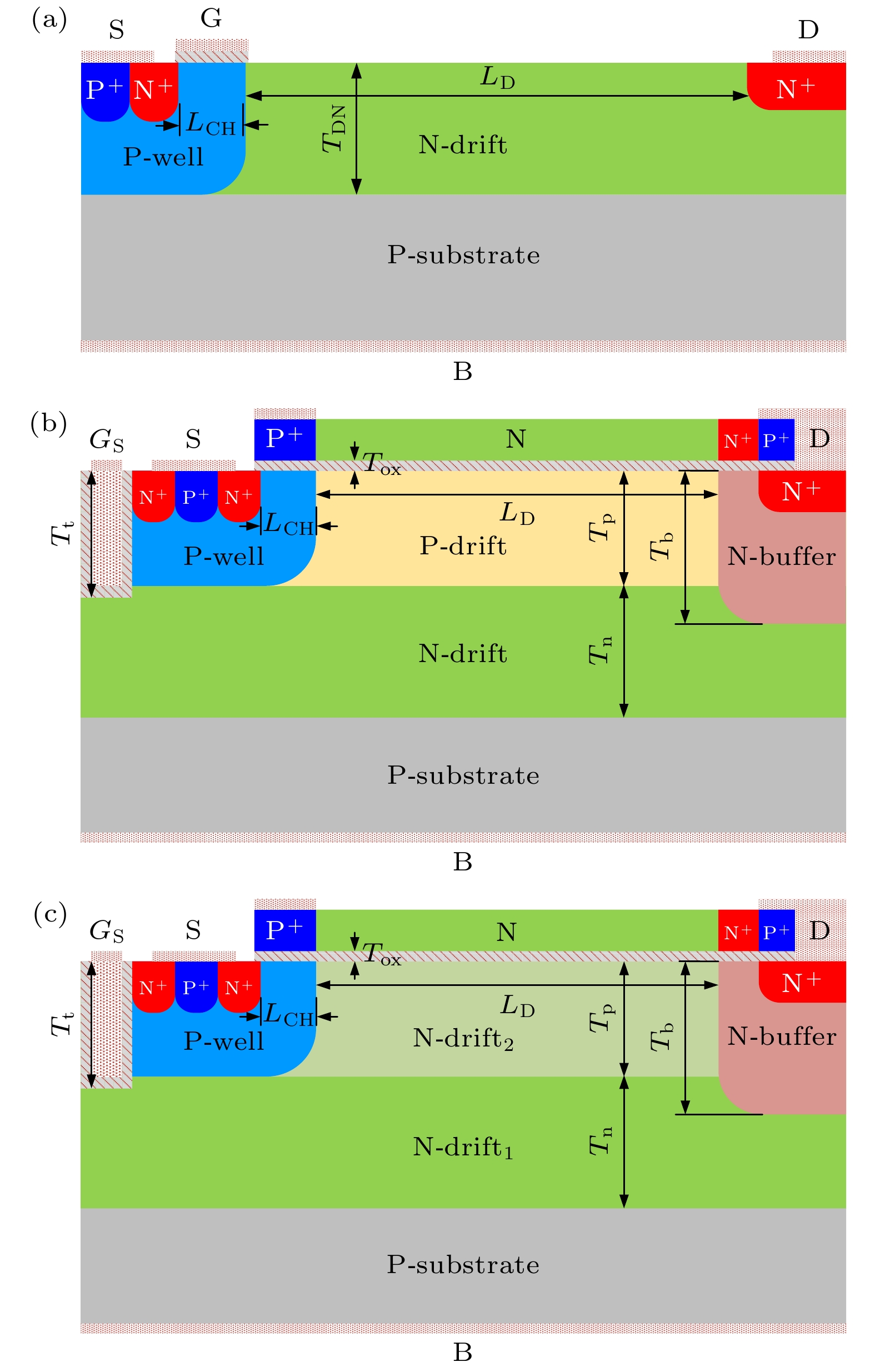
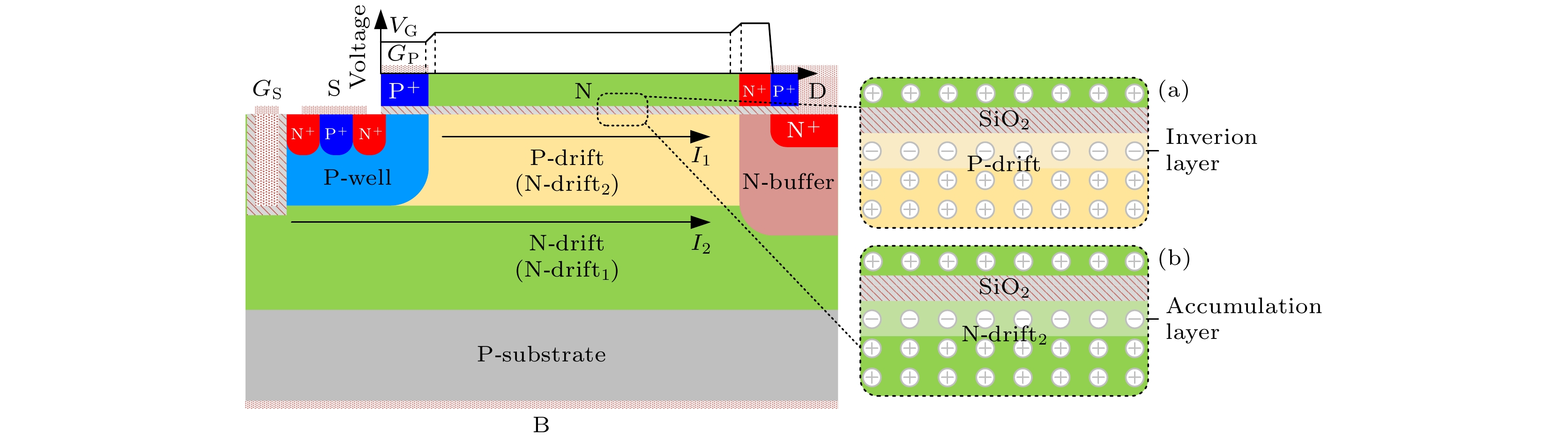
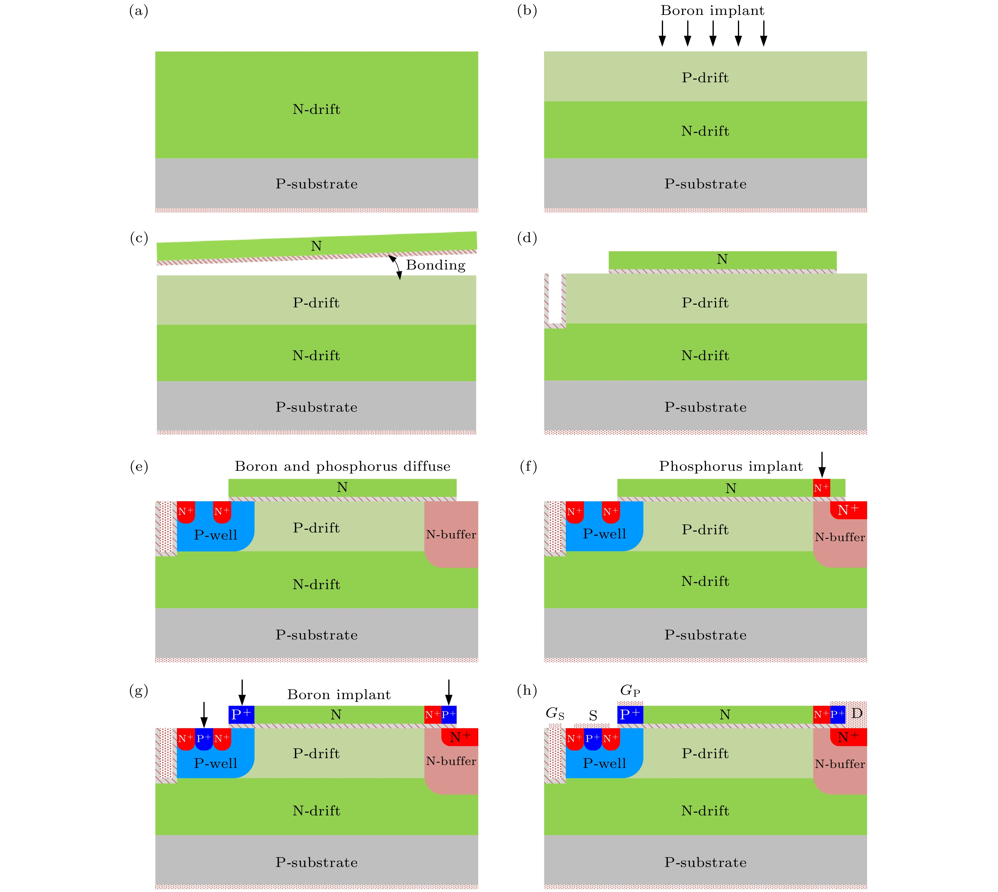
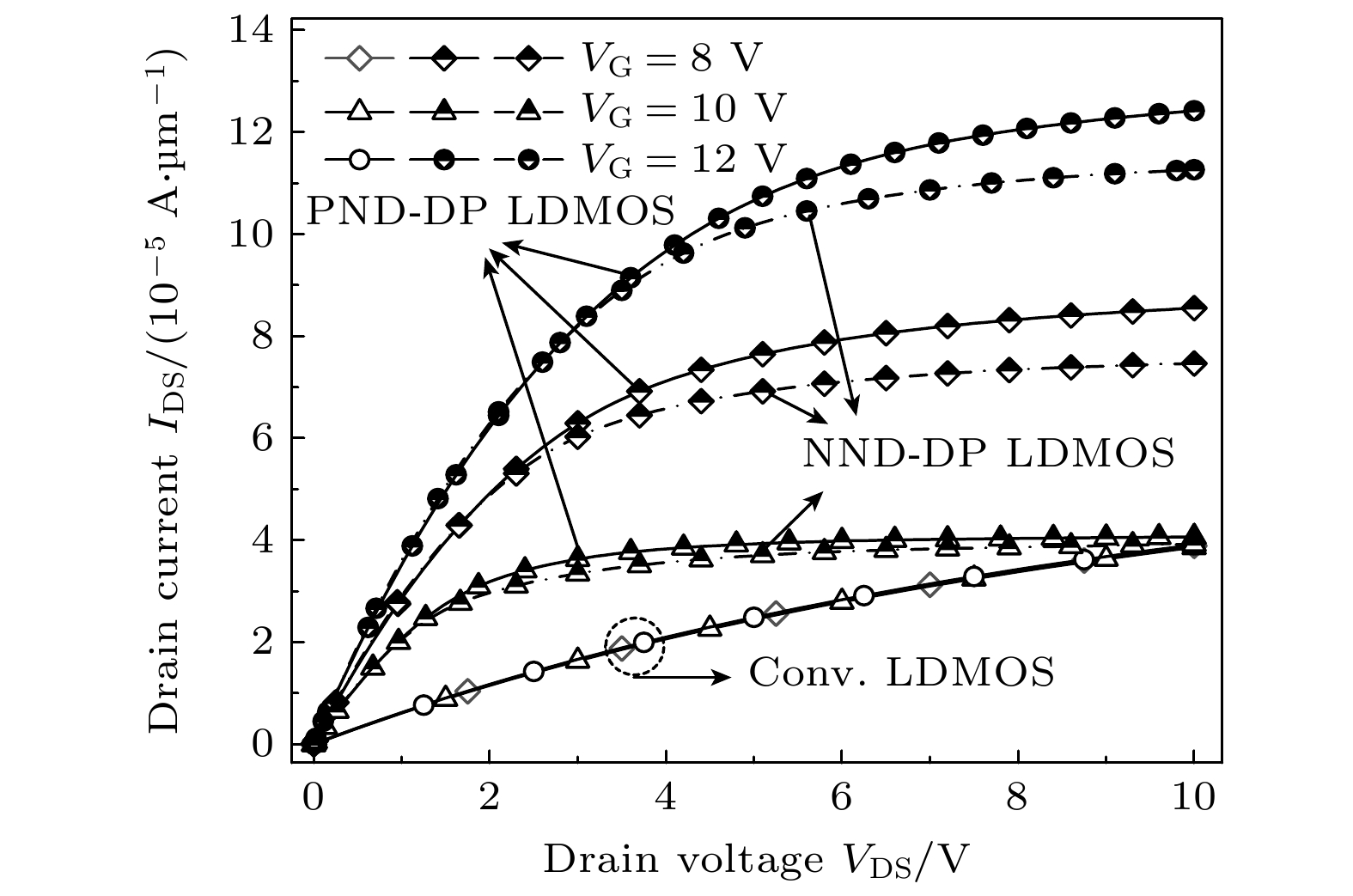
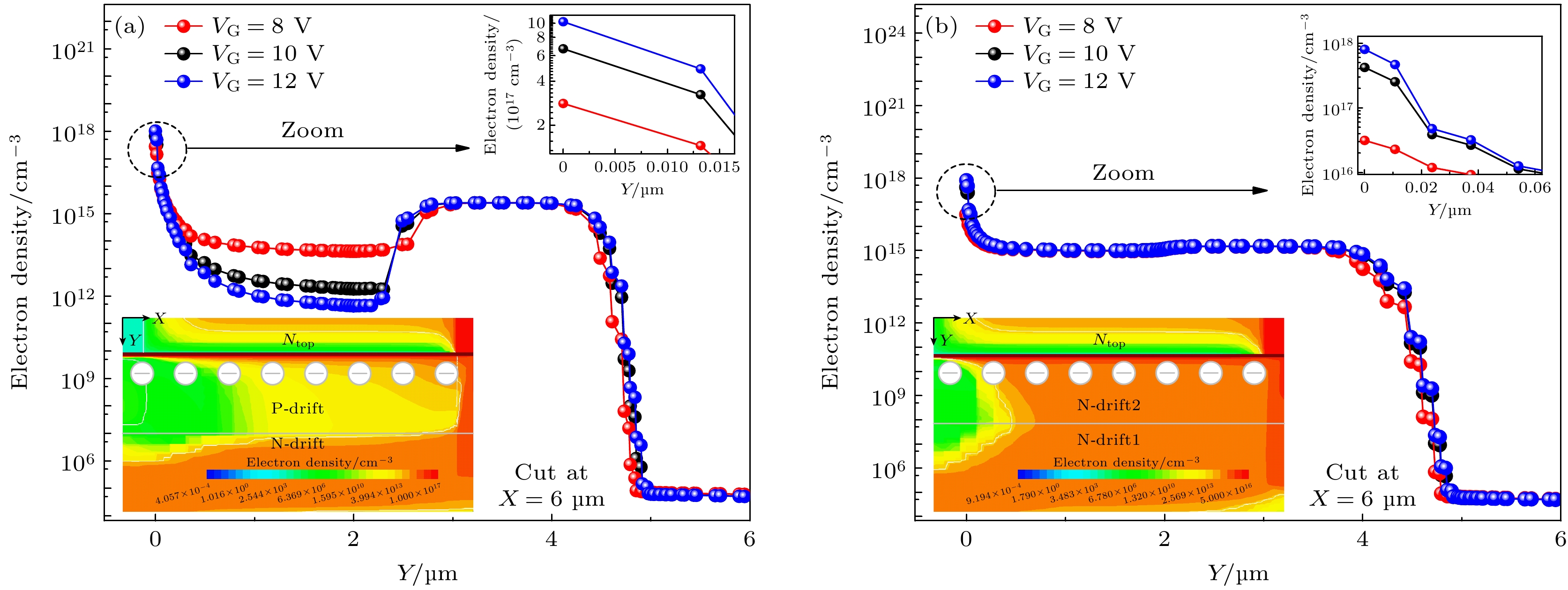
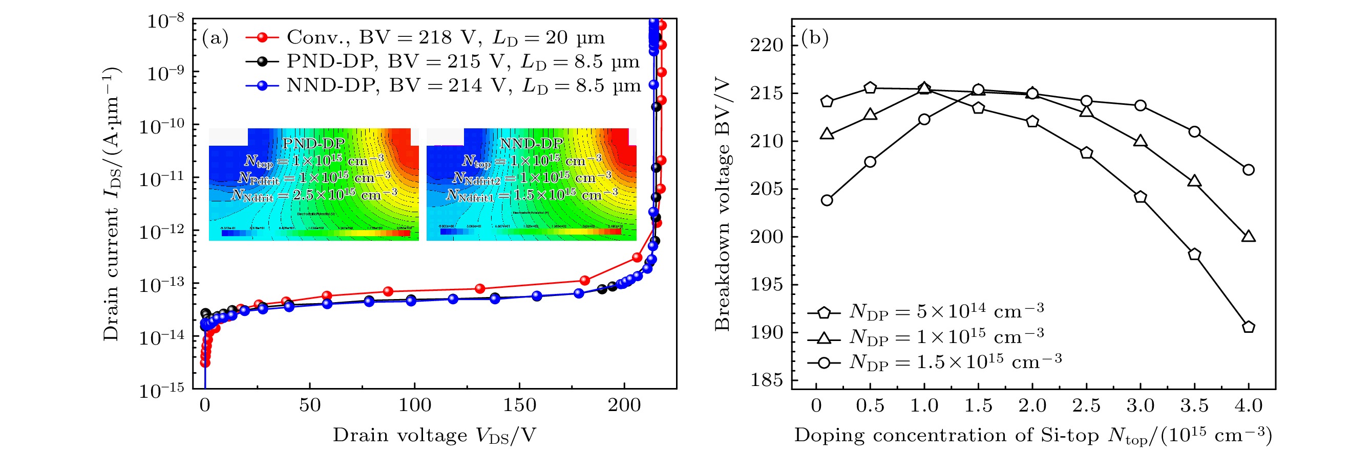
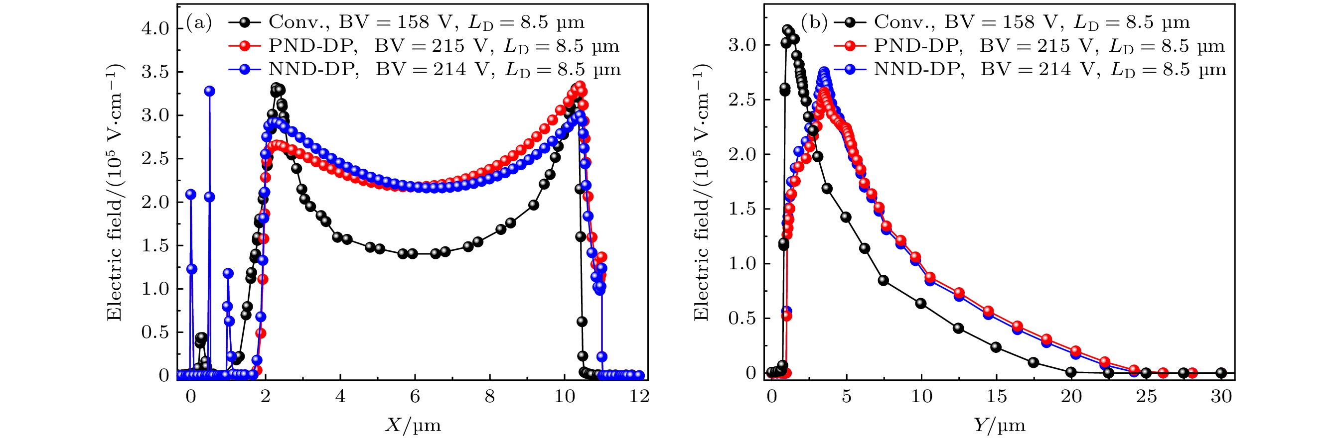
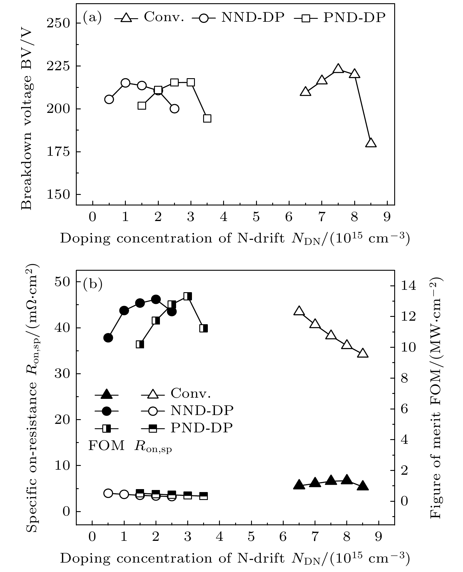
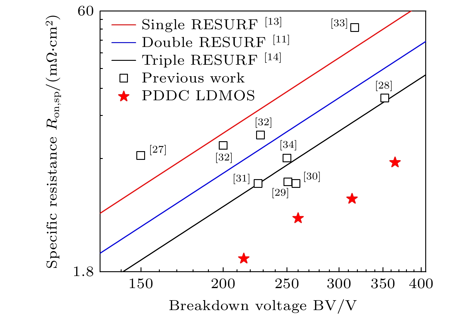
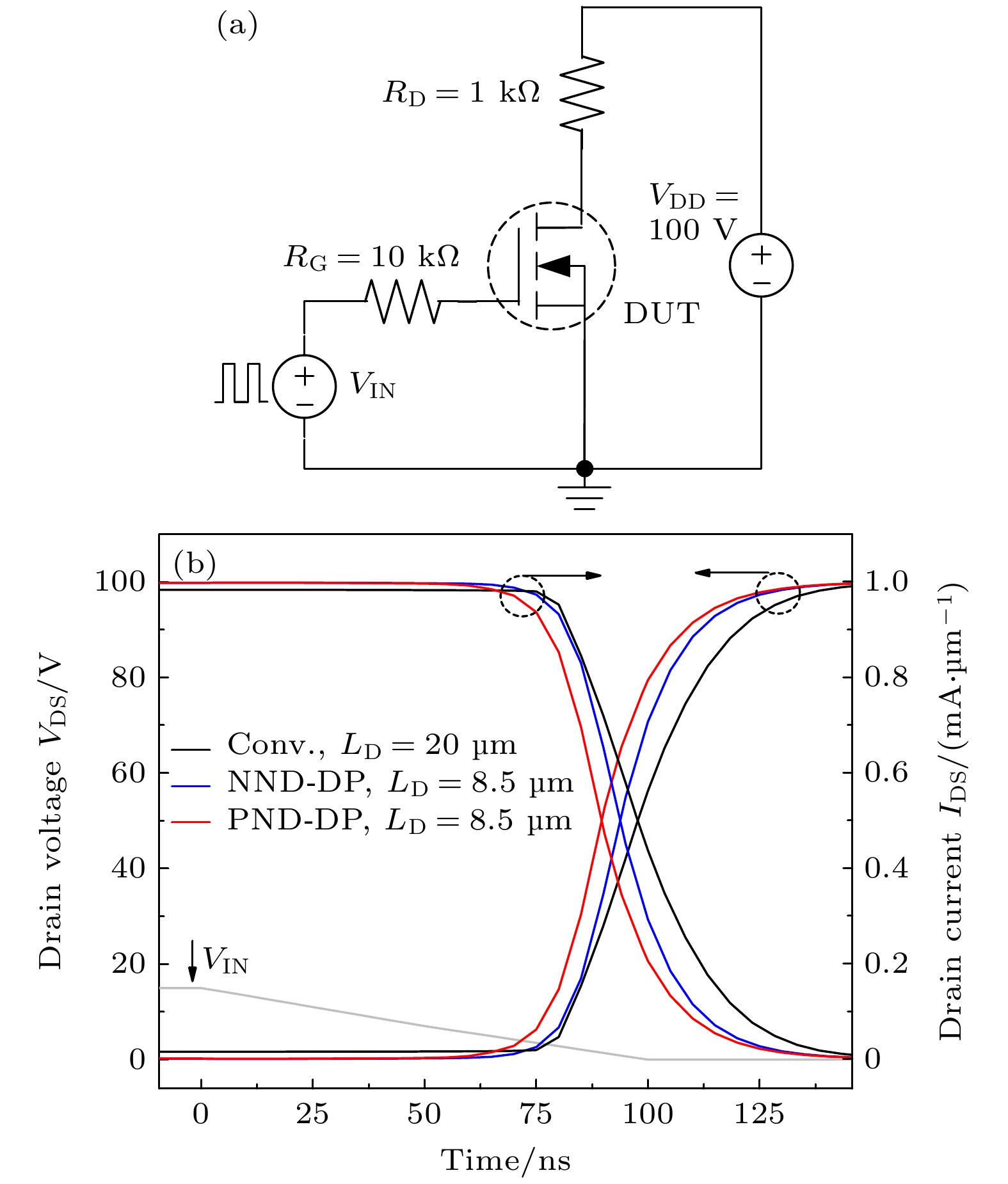
In order to improve the contradictory between specific on-resistance (Ron,sp) and breakdown voltage (BV) of lateral double-diffused metal oxide semiconductor (LDMOS) and enhance the turn-off characteristic, this paper proposes a novel LDMOS device with dual-drift regions and dual-conduction paths, which achieves an ultra-low Ron,sp. The key feature of the proposed device is the introduction of a dual-drift region structure with alternating P-type and N-type regions, combined with planar and trench gates to control the P-type and N-type drift regions, respectively. This configuration enables the formation of two independent electron conduction paths within the drift region. When a positive voltage is applied to the planar gate, a voltage difference is generated between the surface of the P-type drift region and the body of device’s drift. Therefore, under the influence of the voltage difference, the electrons are pulled to the surface of the P-type drift region to invert and form a high-density electron inversion layer that connects the channel and the N+ drain, significantly increasing the electron density during conduction and reducing the Ron,sp. The introduction of the trench gate provides an additional electron disappearance path, which shortens the device's turn-off time (toff). Furthermore, the introduction of the P-type drift region facilitates the recombination of electrons with holes within the P-type drift region, accelerating the electron disappearance process and further reducing the device’s toff. Furthermore, the proposed device exhibits a more uniform electric field distribution and higher voltage capability is due to the P+N-N+P+ structure adopted in the PolySi-top layer. During the off-state, both the P+N- junctions and the N+P+ junctions generate electric field peaks at the interfaces. These peaks modulate the electric field distribution across the surface of the drift region. Simulation results indicate that at the BV with a level of 200V, the proposed LDMOS exhibits an Ron,sp of 3.43 mΩ·cm² and a toff of 9 ns. Compared with conventional LDMOS devices, the proposed LDMOS possesses a 90% reduction in Ron,sp and an 11.6% decrease in toff. The proposed device not only achieves an excellent trade-off between Ron,sp and BV but also shortens the toff, demonstrating that the device achieves superior performance.


 DownLoad: CSV


 DownLoad:


